
Datasheet


Electrical characteristics
i.MX 8QuadXPlus and 8DualXPlus Automotive and Infotainment Applications Processors, Rev. 0, 11/2018
PRELIMINARY NXP Semiconductors80
4.10.8.7 MIPI-DSI DC specifications
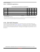
4.10.9 PCIe 3.0 PHY Parameters
The TX and RX eye diagrams specifications are per the template shown in the following figure. The
summary of specifications is shown in Table 76 and Table 77. Note that the time closure (1–A OPENING)
in the eye templates needs not match jitter specifications in the Standards Specifications, as there are such
discrepancies in some Standards Specifications. The design meets the tightest of specifications in case of
discrepancy.
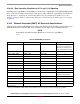
Table 75. MIPI input characteristics DC specifications
Symbol Parameter Min Typ Max Unit
V
PIN
Pad signal voltage range –50 — 1350 mV
I
LEAK
1
1
When the pad voltage is within the signal voltage range between V
GNDSH(min)
to VOH + V
GNDSH(max)
and the Lane Module is
in LP receive mode.
Pin leakage current –10 — 10 μA
V
GNDSH
Ground shift –50 — 50 mV
V
PIN(absmax)
2
2
This value includes ground shift.
Maximum pin voltage level –0.15 — 1.45 V
T
VPIN(absmax)
3
3
The voltage overshoot and undershoot beyond the V
PIN
is only allowed during a single 20 ns window after any LP-0 to LP-1
transition or vice versa. For all other situations it must stay within the V
PIN
range.
Maximum transient time above V
PIN(max)
or below V
PIN(min)
— — 20 ns