
Datasheet


Electrical characteristics
i.MX 8QuadXPlus and 8DualXPlus Automotive and Infotainment Applications Processors, Rev. 0, 11/2018
PRELIMINARYNXP Semiconductors 79
4.10.8.5 MIPI-DSI LP-RX specifications
4.10.8.6 MIPI-DSI LP-CD specifications
3
With an additional load capacitance CCM between 0 to 60 pF on the termination center tap at RX side of the lane.
4
This parameter value can be lower then TLPX due to differences in rise vs. fall signal slopes and trip levels and mismatches
between Dp and Dn LP transmitters. Any LP exclusive-OR pulse observed during HS EoT (transition from HS level to LP-11)
is glitch behavior as described in Low-Power Receiver section.
5
When the output voltage is between 15% and below 85% of the fully settled LP signal levels.
6
Measured as average across any 50 mV segment of the output signal transition.
7
This value represents a corner point in a piecewise linear curve.
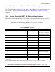
Table 72. MIPI low power receiver DC specifications
Symbol Parameter Min Typ Max Unit
V
IH
Logic 1 input voltage 880 — 1.3 mV
V
IL
Logic 0 input voltage, not in ULP state — — 550 mV
V
IL-ULPS
Logic 0 input voltage, ULP state — — 300 mV
V
HYST
Input hysteresis 25 — — mV
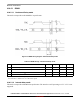
Table 73. MIPI low power receiver AC specifications
Symbol Parameter Min Typ Max Unit
e
SPIKE
1,2
1
Time-voltage integration of a spike above V
IL
when in LP-0 state or below VIH when in LP-1 state.
2
An impulse below this value will not change the receiver state.
Input pulse rejection — — 300 V.ps
T
MIN-RX
3
3
An input pulse greater than this value shall toggle the output.
Minimum pulse width response 20 — — ns
V
INT
Peak Interference amplitude — — 200 mV
f
INT
Interference frequency 450 — — MHz
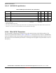
Table 74. MIPI contention detector DC specifications
Symbol Parameter Min Typ Max Unit
V
IHCD
Logic 1 contention threshold 450 — — mV
V
ILCD
Logic 0 contention threshold — — 200 mV