
Datasheet


Electrical characteristics
i.MX 8QuadXPlus and 8DualXPlus Automotive and Infotainment Applications Processors, Rev. 0, 11/2018
PRELIMINARY NXP Semiconductors76
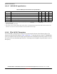
4.10.8 MIPI-DSI/LVDS combo display output specifications
The physical pins of the combo display output controller can be used in LVDS mode or in DSI display
mode.
4.10.8.1 MIPI-DSI/LVDS display bridge module parameters
Maximum frequency support for combination MIPI-DSI/LVDS modules:
Table 66. I2C timing
Fast Mode Plus High Speed
1
1
High-speed mode is only available for I2C modules in DMA, SCU and Cortex-M4 subsystems.
Unit
ID Parameter Min Max Min Max
IC1 SCL clock frequency — 1 — 3.4 MHz
IC2 Hold time (repeated) START condition 260 — 160 — ns
IC3 Set-up time for STOP condition 260 — 160 — ns
IC4 Data hold time 0 — 0 70 ns
IC5 HIGH Period of I2Cx_SCL Clock 260 — 60 — ns
IC6 LOW Period of the I2Cx_SCL Clock 500 — 160 — ns
IC7 Set-up time for a repeated START condition 260 — 160 — ns
IC8 Data set-up time 50 — 10 — ns
IC9 Bus free time between a STOP and START condition 500 — 150 — ns
IC10 Rise time of I2Cx_SDA signals — 120 10 80 ns
IC11 Fall time of I2Cx_SDA signals 12 (@3.3 V)
6.5 (@1.8 V)
120 10 80 ns
IC10b Rise time of I2Cx_SCL signals — 120 10 40 ns
IC11b Fall time of I2Cx_SCL signals 12 (@3.3 V)
6.5 (@1.8 V)
120 10 40 ns
IC12 Capacitive load for each bus line (Cb) — 550 — 100 pF
Function Channel A Channel B
DSI DSI up to 1.05 Gb/per lane DSI up to 1.05 Gb/per lane
Mix 4 pairs LVDS up to 1.05 Gb per pair DSI up to 1.05 Gb/per lane
Mix DSI up to 1.05 Gb/per lane 4 pairs LVDS up to 1.05 Gb per pair
LVDS only 4 pairs LVDS up to 1.05 Gb per pair 4 pairs LVDS up to 1.05 Gb per pair
8 pairs LVDS 8 pairs LVDS up to 595 Mb per pair