
Datasheet


Electrical characteristics
i.MX 8QuadXPlus and 8DualXPlus Automotive and Infotainment Applications Processors, Rev. 0, 11/2018
PRELIMINARYNXP Semiconductors 75
4.10.7 I
2
C Module Timing Parameters
This section describes the timing parameters of the I
2
C module. The following figure depicts the timing
of the I
2
C module, and Table 65 lists the I
2
C module timing characteristics.
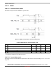
Figure 36. I
2
C bus timing
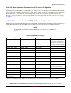
Table 65. I
2
C Module Timing Parameters
ID Parameter
Standard Mode Fast Mode
Unit
Min Max Min Max
IC1 I2Cx_SCL cycle time 10 — 2.5 —
µ
s
IC2 Hold time (repeated) START condition 4.0 — 0.6 —
µ
s
IC3 Set-up time for STOP condition 4.0 — 0.6 —
µ
s
IC4 Data hold time 0
1
1
A device must internally provide a hold time of at least 300 ns for I2Cx_SDA signal in order to bridge the undefined region of
the falling edge of I2Cx_SCL.
3.45
2
2
The maximum hold time has only to be met if the device does not stretch the LOW period (ID no IC5) of the I2Cx_SCL signal.
0
1
0.9
2
µ
s
IC5 HIGH Period of I2Cx_SCL Clock 4.0 — 0.6 —
µ
s
IC6 LOW Period of the I2Cx_SCL Clock 4.7 — 1.3 —
µ
s
IC7 Set-up time for a repeated START condition 4.7 — 0.6 —
µ
s
IC8 Data set-up time 250 — 100
3
3
A Fast-mode I2C-bus device can be used in a Standard-mode I2C-bus system, but the requirement of Set-up time (ID No IC7)
of 250 ns must be met. This automatically is the case if the device does not stretch the LOW period of the I2Cx_SCL signal.
If such a device does stretch the LOW period of the I2Cx_SCL signal, it must output the next data bit to the I2Cx_SDA line
max_rise_time (IC9) + data_setup_time (IC7) = 1000 + 250 = 1250 ns (according to the Standard-mode I2C-bus specification)
before the I2Cx_SCL line is released.
—ns
IC9 Bus free time between a STOP and START condition 4.7 — 1.3 —
µ
s
IC10/IC10b Rise time of both I2Cx_SDA and I2Cx_SCL signals — 1000 20 + 0.1C
b
4
4
C
b
= total capacitance of one bus line in pF.
300 ns
IC11/IC11b Fall time of both I2Cx_SDA and I2Cx_SCL signals — 300 20 + 0.1C
b
4
300 ns
IC12 Capacitive load for each bus line (C
b
) — 400 — 400 pF
IC10
IC11
IC9
IC2
IC8
IC4
IC7
IC3
IC6
IC10b
IC5
IC11b
START
STOP START
START
I2Cx_SDA
I2Cx_SCL
IC1