
Datasheet


Electrical characteristics
i.MX 8QuadXPlus and 8DualXPlus Automotive and Infotainment Applications Processors, Rev. 0, 11/2018
PRELIMINARY NXP Semiconductors70
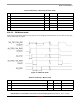
4.10.4.5 SDR50/SDR104 AC Timing
The following figure depicts the timing of SDR50/SDR104, and Table 61 lists the SDR50/SDR104 timing
characteristics.
Figure 32. SDR50/SDR104 timing
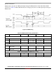
Table 61. SDR50/SDR104 Interface Timing Specification
ID Parameter Symbols Min Max Unit
Card Input Clock
SD1 Clock Frequency Period t
CLK
4.8 — ns
SD2 Clock Low Time t
CL
0.46 × t
CLK
0.54 × t
CLK
ns
SD3 Clock High Time t
CH
0.46 × t
CLK
0.54 × t
CLK
ns
uSDHC Output/Card Inputs SD_CMD, SDx_DATAx in SDR50 (Reference to SDx_CLK)
SD4 uSDHC Output Delay t
OD
–3 1 ns
uSDHC Output/Card Inputs SD_CMD, SDx_DATAx in SDR104 (Reference to SDx_CLK)
SD5
uSDHC Output Delay t
OD
–1.6 1 ns
uSDHC Input/Card Outputs SD_CMD, SDx_DATAx in SDR50 (Reference to SDx_CLK)
SD6
uSDHC Input Setup Time t
ISU
2.5 — ns
SD7
uSDHC Input Hold Time t
IH
1.5 — ns
uSDHC Input/Card Outputs SD_CMD, SDx_DATAx in SDR104 (Reference to SDx_CLK)
1
1
Data window in SDR100 mode is variable.
SD8
Card Output Data Window t
ODW
0.5 × t
CLK
—ns
2XWSXWIURPX6'+&WRFDUG
,QSXWIURPFDUGWRX6'+&
6&.
6'
6'
6'
6'
6'
6'
6'
6'
6'