
Datasheet


Electrical characteristics
i.MX 8QuadXPlus and 8DualXPlus Automotive and Infotainment Applications Processors, Rev. 0, 11/2018
PRELIMINARYNXP Semiconductors 67
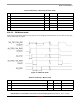
4.10.4.2 eMMC5.1 DDR 52 mode/SD3.1 DDR 50 mode timing
The following figure depicts the timing of eMMC5.1 DDR 52 mode/SD3.1 DDR 50 mode, and Table 58
lists the timing characteristics. Be aware that only SDx_DATA is sampled on both edges of the clock (not
applicable to SD_CMD).
Figure 28. eMMC 5.1 timing
Figure 29. eMMC5.1 DDR 52 mode/SD3.1 DDR 50 mode interface timing
4.10.4.3 HS400 AC timing—eMMC 5.1 only
Figure 30 depicts the timing of HS400. Table 59 lists the HS400 timing characteristics. Be aware that only
data is sampled on both edges of the clock (not applicable to CMD).
The CMD input/output timing for
3
In normal (full) speed mode for MMC card, clock frequency can be any value between 0
–
20 MHz. In high-speed mode, clock
frequency can be any value between 0
–
52 MHz.
4
To satisfy hold timing, the delay difference between clock input and cmd/data input must not exceed 2 ns.
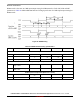
Table 58. eMMC5.1 DDR 52 mode/SD3.1 DDR 50 mode interface timing specification
ID Parameter Symbols Min Max Unit
Card Input Clock
1
1
Clock duty cycle will be in the range of 47% to 53%.
SD1 Clock Frequency (eMMC5.1 DDR) f
PP
052MHz
SD1 Clock Frequency (SD3.1 DDR) f
PP
050MHz
uSDHC Output / Card Inputs SD_CMD, SD
x
_DATA
x
(Reference to CLK)
SD2 uSDHC Output Delay t
OD
2.8 6.8 ns
uSDHC Input / Card Outputs SD_CMD, SD
x
_DATA
x
(Reference to CLK)
SD3 uSDHC Input Setup Time t
ISU
1.7 — ns
SD4 uSDHC Input Hold Time t
IH
1.5 — ns
SD1
SD2
SD3
Output from eSDHCv3 to card
Input from card to eSDHCv3
SDx_DATA[7:0]
SDx_CLK
SD4
SD2
......
......
SDx_DATA[7:0]