
Datasheet


Electrical characteristics
i.MX 8QuadXPlus and 8DualXPlus Automotive and Infotainment Applications Processors, Rev. 0, 11/2018
PRELIMINARY NXP Semiconductors60
4.10.2 Serial audio interface (SAI) timing parameters
The timings and figures in this section are valid for noninverted clock polarity (I2S_TCR2.BCP = 0b0,
I2S_RCR2.BCP = 0b0) and non-inverted frame sync polarity (I2S_TCR4.FSP = 0b0, I2S_RCR4.FSP =
0b0). If the polarity of the clock and/or the frame sync have been inverted, all the timings remain valid by
inverting the clock signal (SAI_TXC / SAI_RXC) and/or the frame sync (SAI_TXFS / SAI_RXFS) shown
in the figures below.
The same performance is achieved at both 1.8 V and 3.3 V unless otherwise stated.
NOTE
SAI0 and SAI1 are transmit/receive capable. SAI2 and SAI3 are receive only.
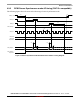
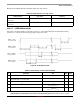
4.10.2.1 SAI Master Synchronous mode
In this mode, transmitter clock and frame sync are used by both transmitter and receiver
(I2S_TCR2.SYNC=0b00, I2S_RCR2.SYNC=0b01). In that case, SAI interface requires only 4 signals to
be routed: SAI_TXC, SAI_TXFS, SAI_TXD and SAI_RXD. SAI_RXC and SAI_RXFS can be left
unconnected. I2S_RCR2.BCI shall be set to 0b1 to get setup and hold times provided in Table 1.
Figure 22. SAI Master Synchronous mode
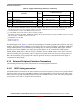
t4 SPI
x
_CSy Lag Time (CS hold time) 2 — ns
t5 SPI
x
_SDO output Delay (CLOAD = 20 pF) — 18 ns
t6 SPI
x
_SDI Setup Time 2 — ns
t7 SPI
x
_SDI Hold Time 2 — ns
Table 52. LPSPI timings—Slave mode at 20 MHz (continued)
ID Parameter Min Max Unit