
Datasheet


Electrical characteristics
i.MX 8QuadXPlus and 8DualXPlus Automotive and Infotainment Applications Processors, Rev. 0, 11/2018
PRELIMINARY NXP Semiconductors58
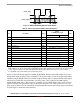
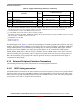
t5 SPIx_SDO output Delay (CLOAD = 20 pF) — 3 ns
t6 SPIx_SDI Setup Time 2 — ns
t7 SPIx_SDI Hold Time 2 — ns
1
This timing is controllable through CCR.PCSSCK and TCR.PRESCALE registers.
2
FCLK_PERIOD is the period of the functional clock provided to LPSPI module. Maximum allowed frequency is 240 MHz.
3
This timing is controllable through CCR.SCKPCS and TCR.PRESCALE registers.
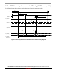
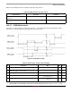
Table 50. LPSPI timings—Master mode at 40 MHz
ID Parameter Min Max Unit
— SPIx_SCLK Cycle frequency — 40 MHz
t1 SPIx_SCLK High or Low Time–Read
SPIx_SCLK High or Low Time–Write
11 — ns
t2 SPIx_CSy pulse width 11 — ns
t3 SPIx_CSy Lead Time
(1)
1
This timing is controllable through CCR.PCSSCK and TCR.PRESCALE registers.
FCLK_PERIOD
(2)
x (PCSSCK
+ 1) / 2
PRESCALE
+ 3
2
FCLK_PERIOD is the period of the functional clock provided to LPSPI module. Maximum allowed frequency is 240 MHz.
—ns
t4 SPIx_CSy Lag Time
(3)
3
This timing is controllable through CCR.SCKPCS and TCR.PRESCALE registers.
FCLK_PERIOD
(2)
x (SCKPCS
+ 1) / 2
PRESCALE
+ 3
—ns
t5 SPIx_SDO output Delay (CLOAD = 20 pF) — 5 ns
t6 SPIx_SDI Setup Time 5 — ns
t7 SPIx_SDI Hold Time 4 — ns
Table 49. LPSPI timings—Master mode at 60 MHz (continued)
ID Parameter Min Max Unit