
Datasheet


Electrical characteristics
i.MX 8QuadXPlus and 8DualXPlus Automotive and Infotainment Applications Processors, Rev. 0, 11/2018
PRELIMINARY NXP Semiconductors56
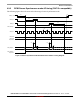
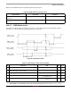
For DDR Toggle mode, Figure 17 shows the timing diagram of NAND_DQS/NAND_DATAxx read valid
window. The typical value of tDQSQ is 1.4 ns (max) and 1.4 ns (max) for tQHS at 133 MB/s. GPMI will
sample NAND_DATA[7:0] at both rising and falling edge of an delayed NAND_DQS signal, which is
provided by an internal DPLL. The delay value of this register can be controlled by GPMI register
GPMI_READ_DDR_DLL_CTRL.SLV_DLY_TARGET (see the GPMI chapter of the device reference
manual. Generally, the typical delay value is equal to 0x7 which means 1/4 clock cycle delay expected.
But if the board delay is big enough and cannot be ignored, the delay value should be made larger to
compensate the board delay.
4.10 External Peripheral Interface Parameters
The following subsections provide information on external peripheral interfaces.
4.10.1 LPSPI timing parameters
All LPSPI interfaces do not have the same maximum serial clock frequency. There are two groups. LPSPI
interfaces which can operate at 60 MHz in Master mode and 40 MHz in Slave mode and the other group
where interfaces operate at 40 MHz in Master mode and 20 MHz in Slave mode. The same performance
is achieved at 1.8 V and 3.3 V unless otherwise stated.
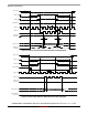
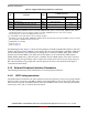
NF28 Data write setup tDS
6
0.25 × tCK - 0.32 — ns
NF29 Data write hold tDH
6
0.25 × tCK - 0.79 — ns
NF30 NAND_DQS/NAND_DQ read setup skew tDQSQ
7
—3.18
NF31 NAND_DQS/NAND_DQ read hold skew tQHS
7
—3.27
1
The GPMI toggle mode output timing can be controlled by the module’s internal registers
HW_GPMI_TIMING0_ADDRESS_SETUP, HW_GPMI_TIMING0_DATA_SETUP, and HW_GPMI_TIMING0_DATA_HOLD.
This AC timing depends on these registers settings. In the table, AS/DS/DH represents each of these settings.
2
AS minimum value can be 0, while DS/DH minimum value is 1.
3
T = tCK (GPMI clock period) -0.075 ns (half of maximum p-p jitter).
4
CE_DELAY represents HW_GPMI_TIMING2[CE_DELAY]. NF18 is guaranteed by the design. Read/Write operation is started
with enough time of ALE/CLE assertion to low level.
5
PRE_DELAY+1)
≥
(AS+DS)
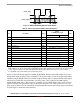
6
Shown in Figure 18.
7
Shown in Figure 19.
Table 47. Toggle mode timing parameters
1
(continued)
ID Parameter Symbol
Timing
T = GPMI Clock Cycle
Unit
Min. Max.