
Datasheet


Electrical characteristics
i.MX 8QuadXPlus and 8DualXPlus Automotive and Infotainment Applications Processors, Rev. 0, 11/2018
PRELIMINARY NXP Semiconductors54
4.9.3 ONFI NV-DDR2 mode (ONFI 3.2 compatible)
4.9.3.1 Command and address timing
ONFI 3.2 mode command and address timing is the same as ONFI 1.0 compatible Async mode AC timing.
See Section 4.9.1, “GPMI Asynchronous mode AC timing (ONFI 1.0 compatible),” for details.
4.9.3.2 Read and write timing
ONFI 3.2 mode read and write timing is the same as Toggle mode AC timing. See Section 4.9.4, “Toggle
mode AC Timing,” for details.
4.9.4 Toggle mode AC Timing
4.9.4.1 Command and address timing
NOTE
Toggle mode command and address timing is the same as ONFI 1.0
compatible Asynchronous mode AC timing. See Section 4.9.1, “GPMI
Asynchronous mode AC timing (ONFI 1.0 compatible),” for details.
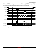
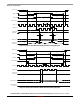
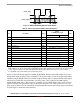
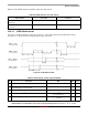
4.9.4.2 Read and write timing
Figure 18. Toggle mode data write timing