
Datasheet


Electrical characteristics
i.MX 8QuadXPlus and 8DualXPlus Automotive and Infotainment Applications Processors, Rev. 0, 11/2018
PRELIMINARYNXP Semiconductors 53
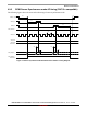
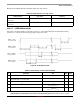
Figure 17. NAND_DQS/NAND_DQ Read Valid Window
Figure 17 shows the timing diagram of NAND_DQS/NAND_DATAxx read valid window. For Source
Synchronous mode, the typical value of tDQSQ is 0.85 ns (max) and 1 ns (max) for tQHS at 200 MB/s.
GPMI will sample NAND_DATA[7:0] at both rising and falling edge of a delayed NAND_DQS signal,
which can be provided by an internal DPLL. The delay value can be controlled by GPMI register
GPMI_READ_DDR_DLL_CTRL.SLV_DLY_TARGET (see the GPMI chapter of the device reference
manual. Generally, the typical delay value of this register is equal to 0x7 which means 1/4 clock cycle
delay expected. However, if the board delay is large enough and cannot be ignored, the delay value should
be made larger to compensate the board delay.
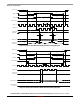
Table 46. Source Synchronous Mode Timing Parameters
1
1
The GPMI source synchronous mode output timing can be controlled by the module’s internal registers
GPMI_TIMING2_CE_DELAY, GPMI_TIMING_PREAMBLE_DELAY, GPMI_TIMING2_POST_DELAY. This AC timing depends
on these registers settings. In the table, CE_DELAY/PRE_DELAY/POST_DELAY represents each of these settings.
ID Parameter Symbol
Timing
T = GPMI Clock Cycle
Unit
Min Max
NF18 NAND_CEx_B access time tCE CE_DELAY × T - 0.79 [see
2
]
2
T = tCK (GPMI clock period) -0.075ns (half of maximum p-p jitter).
ns
NF19 NAND_CEx_B hold time tCH 0.5 × tCK - 0.63 [see
2
]ns
NF20 Command/address NAND_DATAxx setup time tCAS 0.5 × tCK - 0.05 ns
NF21 Command/address NAND_DATAxx hold time tCAH 0.5 × tCK - 1.23 ns
NF22 clock period tCK — ns
NF23 preamble delay tPRE PRE_DELAY × T - 0.29 [see
2
]ns
NF24 postamble delay tPOST POST_DELAY × T - 0.78 [see
2
]ns
NF25 NAND_CLE and NAND_ALE setup time tCALS 0.5 × tCK - 0.86 ns
NF26 NAND_CLE and NAND_ALE hold time tCALH 0.5 × tCK - 0.37 ns
NF27 NAND_CLK to first NAND_DQS latching transition tDQSS T - 0.41 [see
2
]ns
NF28 Data write setup tDS 0.25 × tCK - 0.35 ns
NF29 Data write hold tDH 0.25 × tCK - 0.85 ns
NF30 NAND_DQS/NAND_DQ read setup skew tDQSQ — 2.06 —
NF31 NAND_DQS/NAND_DQ read hold skew tQHS — 1.95 —
Ϭ ϭ Ϯ ϯ
.!.$?$13
.!.$?$!4!;=
E&ϯϬ
E&ϯϭ
E&ϯϬ
E&ϯϭ