
Datasheet


Electrical characteristics
i.MX 8QuadXPlus and 8DualXPlus Automotive and Infotainment Applications Processors, Rev. 0, 11/2018
PRELIMINARY NXP Semiconductors50
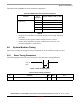
In EDO mode (Figure 13), NF16/NF17 are different from the definition in non-EDO mode (Figure 12).
They are called tREA/tRHOH (NAND_RE_B access time/NAND_RE_B HIGH to output hold). The
typical value for them are 16 ns (max for tREA)/15 ns (min for tRHOH) at 50 MB/s EDO mode. In EDO
mode, GPMI will sample NAND_DATAxx at rising edge of delayed NAND_RE_B provided by an
internal DPLL. The delay value can be controlled by GPMI_CTRL1.RDN_DELAY (see the GPMI chapter
of the device reference manual. The typical value of this control register is 0x8 at 50 MT/s EDO mode.
However, if the board delay is large enough and cannot be ignored, the delay value should be made larger
to compensate the board delay.
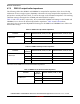
NF16 Data setup on read tDSR — (DS × T -0.67)/18.38 [see
5,6
]ns
NF17 Data hold on read tDHR 0.82/11.83 [see
5,6
]—ns
1
The GPMI asynchronous mode output timing can be controlled by the module’s internal registers
HW_GPMI_TIMING0_ADDRESS_SETUP, HW_GPMI_TIMING0_DATA_SETUP, and HW_GPMI_TIMING0_DATA_HOLD.
This AC timing depends on these registers settings. In the table, AS/DS/DH represents each of these settings.
2
AS minimum value can be 0, while DS/DH minimum value is 1.
3
T = GPMI clock period -0.075ns (half of maximum p-p jitter).
4
NF12 is met automatically by the design.
5
Non-EDO mode.
6
EDO mode, GPMI clock ≈ 100 MHz
(AS=DS=DH=1, GPMI_CTL1 [RDN_DELAY] = 8, GPMI_CTL1 [HALF_PERIOD] = 0).
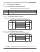
Table 45. Asynchronous Mode Timing Parameters
1
(continued)
ID Parameter Symbol
Timing
T = GPMI Clock Cycle
Unit
Min Max