
Datasheet


Electrical characteristics
i.MX 8QuadXPlus and 8DualXPlus Automotive and Infotainment Applications Processors, Rev. 0, 11/2018
PRELIMINARYNXP Semiconductors 45
www.nxp.com/products/processors-and-microcontrollers/applications-processors/i.mx-applications-proc
essors/i.mx-8-processors:IMX8-SERIES.
Processors that demonstrate full DDR performance on NXP validated designs, but do not function on
customer designs, are not considered marginal parts. A report detailing how the returned part behaved on
an NXP validated system will be provided to the customer as closure to a customer’s reported DDR issue.
Customers bear the responsibility of properly designing the Printed Circuit Board, correctly simulating and
modeling the designed DDR system, and validating the system under all expected operating conditions
(temperatures, voltages) prior to releasing their product to market.
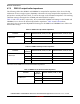
4.8.3.1 Clock/data/command/address pin allocations
These processors uses generic names for clock, data and command address bus (DCF—DRAM controller
functions); the following table provides mapping of clock, data and command address signals for LPDDR4
and DDR3L modes.
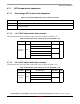
Table 43. i.MX 8QuadXPlus/8DualXPlus DRAM controller supported SDRAM configurations
Parameter LPDDR4 DDR3L
Number of Controllers 1
Number of Channels 2 per controller N/A
Number of Chip Selects 2 per channel 2 per controller
Bus Width 16-bit per channel 32-bit (optional 40-bit with ECC)
Maximum Clock Frequency 1200 MHz 933 MHz
Table 44. Clock, data, and command address signals for LPDDR4 and DDR3L modes
Signal name
DDR3L LPDDR4
DDR_CK0_P CK_t CK_t_A
DDR_CK0_N CK_c CK_c_A
DDR_CK1_P CK_t_B
DDR_CK1_N CK_c_B
DDR_DQ_[15:0] DQ[15:0] DQ[15:0]_A
DDR_DQ_[31:16] DQ[31:16] DQ[15:0]_B
DDR_DQ_[39:32] DQ[39:32]
DDR_DQS_N_[3:0] DQS_N_[3:0] DQS_N_[3:0]
DDR_DQS_P_[3:0] DQS_P_[3:0] DQS_P_[3:0]
DDR_DQS_N_4 DQS_N_4
DDR_DQS_P_4 DQS_P_4
DDR_DM_[3:0] DM_[3:0] DM_[3:0]