
Datasheet


Electrical characteristics
i.MX 8QuadXPlus and 8DualXPlus Automotive and Infotainment Applications Processors, Rev. 0, 11/2018
PRELIMINARY NXP Semiconductors44
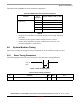
4.8.2 WDOG reset timing parameters
The following figure shows the WDOG reset timing and Table 42 lists the timing parameters.
Figure 8. SCU_WDOG_OUT timing diagram
NOTE
XTALOSC_RTC_XTALI is approximately 32 kHz.
XTALOSC_RTC_XTALI cycle is one period or approximately 30 μs.
4.8.3 DDR SDRAM–specific parameters (LPDDR4 and DDR3L)
The i.MX 8x Family of processors have been designed and tested to work with JEDEC
JESD209-4A–compliant LPDDR4 memory and with JEDEC JESD79-3-1 DDR3L compliant with
DDR3L memory. Timing diagrams and tolerances required to work with these memories are specified in
the respective documents and are not reprinted here.
Meeting the necessary timing requirements for a DDR memory system is highly dependent on the
components chosen and the design layout of the system as a whole. NXP cannot cover in this document
all the requirements needed to achieve a design that meets full system performance over temperature,
voltage, and part variation; PCB trace routing, PCB dielectric material, number of routing layers used,
placement of bulk/decoupling capacitors on critical power rails, VIA placement, GND and Supply planes
layout, and DDR controller/PHY register settings all are factors affecting the performance of the memory
system. Consult the hardware user guide for this device and NXP validated design layouts for information
on how to properly design a PCB for best DDR performance. NXP strongly recommends duplicating an
NXP validated design as much as possible in the design of critical power rails, placement of
bulk/decoupling capacitors and DDR trace routing between the processor and the selected DDR memory.
All supporting material is readily available on the device web page on
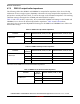
Table 42. WDOG1_B timing parameters
ID Parameter Min Max Unit
CC3 Duration of SCU_WDOG_OUT assertion 1 — XTALOSC_RTC_ XTALI cycle