
Datasheet


Electrical characteristics
i.MX 8QuadXPlus and 8DualXPlus Automotive and Infotainment Applications Processors, Rev. 0, 11/2018
PRELIMINARY NXP Semiconductors42
4.7.2 DDR I/O output buffer impedance
The following tables show DDR3L and LPDDR4 I/O output buffer impedance of the device.The ZQ
Calibration cell uses a single register (ZQnPR0) to determine the target output buffer impedances of the
pull-up driver and the pull-down driver, as well as the target on-die termination impedance. The resulting
calibration setting is then applied to all DDR pads within the PHY complex.
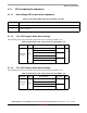
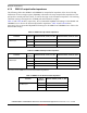
Table 37 and Table 38 show, respectively, the recommended ZQnPR0 field settings for the DDR3L and
LPDDR4 I/O’s to achieve the desired output buffer impedances. Table 39 and Table 40 show,
respectively, the recommended ZQnPR0 field settings for the DDR3L and LPDDR4 I/Os to achieve the
desired ODT settings.
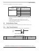
This table shows DDR3L I/O on-die termination impedance.
Table 37. DDR3L I/O output buffer impedance
Parameter
Typical
Impedance
ZQnPR0. ZPROG_ASYM_PU_DRV ZQnPR0. ZPROG_ASYM_PU_DRV
Recommended combinations
for DQ/CA pins
48.0 Ω 99
40.0 Ω 11 11
34.3 Ω 13 13
Table 38. LPDDR4 I/O output buffer impedance
Parameter
Typical
Impedance
ZQnPR0. ZPROG_ASYM_PU_DRV ZQnPR0. ZPROG_ASYM_PU_DRV
Recommended combinations
for DQ/CA pins
80.0 Ω 53
60.0 Ω 75
48.0 Ω 97
40.0 Ω 11 9
Table 39. DDR3L I/O on-die termination impedance
Parameter
Typical
Impedance
ZQnPR0. ZPROG_ASYM_PU_DRV
Recommended combinations
for DQ/CA pins
120.0 Ω 1
60.0 Ω 3
40.0 Ω 5