
Datasheet


Electrical characteristics
i.MX 8QuadXPlus and 8DualXPlus Automotive and Infotainment Applications Processors, Rev. 0, 11/2018
PRELIMINARY NXP Semiconductors40
NOTE
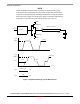
GPIO and DDR I/O output driver impedance is measured with “long”
transmission line of impedance Ztl attached to I/O pad and incident wave
launched into transmission line. Rpu/Rpd and Ztl form a voltage divider that
defines specific voltage of incident wave relative to OVDD. Output driver
impedance is calculated from this voltage divider (see Figure 6).
Figure 6. Impedance Matching Load for Measurement
ipp_do
Cload = 1p
Ztl
Ω
, L = 20 inches
predriver
PMOS (Rpu)
NMOS (Rpd)
pad
OVDD
OVSS
t,(ns)
U,(V)
OVDD
t,(ns)
0
VDD
Vin
(do)
Vout (pad)
U,(V)
Vref
Rpu =
Vovdd – Vref1
Vref1
×
Ztl
Rpd =
×
Ztl
Vref2
Vovdd – Vref2
Vref1
Vref2
0