
Datasheet


Electrical characteristics
i.MX 8QuadXPlus and 8DualXPlus Automotive and Infotainment Applications Processors, Rev. 0, 11/2018
PRELIMINARYNXP Semiconductors 39
4.7 Output Buffer Impedance Parameters
This section defines the I/O impedance parameters for the following I/O types:
• General Purpose I/O (GPIO) output buffer impedance
• Double Data Rate I/O (DDR) output buffer impedance for LPDDR4 and DDR3L modes
f
max
Maximum frequency Load = 30 pF — — 52 MHz
tr Rise time Measured between
V
OL
and V
OH
—— 3 ns
tf Fall time Measured between
V
OH
and V
OL
—— 3 ns
1
All output I/O specifications are guaranteed for Accurate mode of the compensation cell operation. This is applicable for both
DC and AC specifications.
2
All timing specifications in 1.8 V application are valid for High Drive mode (PDRV = H). In Low Drive mode (PDRV = L), the
driver is functional.
3
All timing specifications in 3.3 V application are valid for Type B driver only. In Type A, the driver is functional.
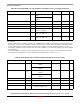
Table 33. Dynamic input characteristics
Symbol Parameter Condition
1,2
1
For all supply ranges of operation.
2
The dynamic input characteristic specifications are applicable for the digital bidirectional cells.
Min Max Unit
Dynamic Input Characteristics for 3.3 V Application
f
op
Input frequency of operation — — 52 MHz
INPSL Slope of input signal at I/O Measured between 10% to 90% of the I/O swing — 3.5 ns
IOMAX High level input voltage — 0.9 * 3.3 V 3.3 V + 0.3 V V
IOMIN Low level input voltage — -0.3 V 0.1 * 3.3 V
Dynamic Input Characteristics for 1.8 V Application
f
op
Input frequency of operation — — 208 MHz
INPSL Slope of input signal at I/O Measured between 10% to 90% of the I/O swing — 1.5 ns
IOMAX High level input voltage — 0.9 * 1.8 V 1.8 V + 0.3 V V
IOMIN Low level input voltage — -0.3 V 0.1 * 1.8 V
Table 32. General Purpose I/O AC Parameters
1
(continued)
Symbol Parameter Test Condition Min Typ Max Unit