
Datasheet


Electrical characteristics
i.MX 8QuadXPlus and 8DualXPlus Automotive and Infotainment Applications Processors, Rev. 0, 11/2018
PRELIMINARY NXP Semiconductors38
4.6 I/O AC Parameters
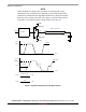
The GPIO and DDR I/O load circuit and output transition time waveforms are shown in Figure 4 and
Figure 5.
Figure 4. Load Circuit for Output
Figure 5. Output Transition Time Waveform
4.6.1 General Purpose I/O (GPIO) AC Parameters
Input current (no ODT) I
IN
V
I
= VSSQ, V
I
= VDDQ -2 2 μA
DC High-Level input voltage V
IH_DC
VREF + 0.09 VDDQ V
DC Low-Level input voltage V
IL_DC
VSSQ VREF – 0.09 V
1
Maximum peak amplitude allowed for overshoot and undershoot area = 0.35 V. Maximum overshoot area above VDD/VDDQ
0.8 V-ns; maximum undershoot area below VSS/VSSQ 0.8 V-ns.
Table 32. General Purpose I/O AC Parameters
1
Symbol Parameter Test Condition Min Typ Max Unit
1.8 V application
2
f
max
Maximum frequency Load = 21 pF (PDRV = H, high
drive, Type A, 33 Ω
— — 208 MHz
Load = 15 pF (PDRV = L, low
drive, Type B, 50 Ω
tr Rise time Measured between V
OL
and
V
OH
0.4 — 1.32 ns
tf Fall time Measured between V
OH
and
V
OL
0.4 — 1.32 ns
Driver 3.3 V application
3
Table 31. SSTL DDR3L DC parameters (continued)
Parameter Symbol Test Conditions Min Max Units
Test Point
From Output
CL
CL includes package, probe and fixture capacitance
Under Test
0V
OVDD
20%
80%
80%
20%
tr
tf
Output (at pad)