
Datasheet


Electrical characteristics
i.MX 8QuadXPlus and 8DualXPlus Automotive and Infotainment Applications Processors, Rev. 0, 11/2018
PRELIMINARYNXP Semiconductors 37
4.5.3 DDR I/O DC parameters
The DDR I/O pads support LPDDR4 and DDR3L operational modes.
4.5.3.1 LPDDR4 mode I/O DC parameters
These parameters are guaranteed per the operating ranges in Table 6 unless otherwise noted.
4.5.3.2 DDR3L mode I/O DC parameters
3
To maintain a valid level, the transition edge of the input must sustain a constant slew rate (monotonic) from the current DC
level through to the target DC level, V
IL
or V
IH
. Monotonic input transition time is from 0.1 ns to 1 ns.
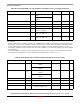
Table 30. LPDDR4 DC parameters
Parameter Symbol Test Conditions Min Max Units
High-level output voltage
1
1
Maximum peak amplitude allowed for overshoot and undershoot area = 0.35 V. Maximum overshoot area above VDD/VDDQ
0.8 V-ns; maximum undershoot area below VSS/VSSQ 0.8 V-ns.
V
OH
Out Drive = All setting
(40,48,60,80,120,240)
unterminated outputs loaded
with 1pF capacitor load
0.9 × V
DDQ
—V
Low-level output voltage
1
V
OL
Out Drive = All setting
(40,48,60,80,120,240)
unterminated outputs loaded
with 1pF capacitor load
—0.1× V
DDQ
V
Input current (no ODT) I
IN
V
I
= VSSQ, V
I
= VDDQ -2 2 μA
DC High-Level input voltage V
IH_DC
— VREF + 0.1 VDDQ V
DC Low-Level input voltage V
IL_DC
— VSSQ VREF – 0.1 V
Table 31. SSTL DDR3L DC parameters
Parameter Symbol Test Conditions Min Max Units
DC High-level output voltage
1
V
OH
Out Drive = All setting
(40,60,120) unterminated
outputs loaded with 1pF
capacitor load
0.8 × V
DDQ
—V
DC Low-level output voltage
1
V
OL
Out Drive = All setting
(40,60,120) unterminated
outputs loaded with 1pF
capacitor load
—0.2× V
DDQ
V
Input termination resistance (ODT) to VDDQ/2 RTT 40 Ω setting 36 44 Ω
60 Ω setting 54 66
120 Ω setting 100 140