
Datasheet


Electrical characteristics
i.MX 8QuadXPlus and 8DualXPlus Automotive and Infotainment Applications Processors, Rev. 0, 11/2018
PRELIMINARYNXP Semiconductors 35
4.5.2.2 Single-voltage GPIO DC parameters
Table 28 and Table 29 show single-voltage 1.8 V and 3.3 V DC parameters, respectively, for GPIO pads.
These parameters are guaranteed per the operating ranges in Table 6 unless otherwise noted.
Pull-down resistance R
down
Vin=OVDD( Pulldown Resistor)
PUN = "H", PDN = "L"
10 100 kΩ
Input current (no PU/PD) I
IN
V
I
= 0, V
I
= OVDD
PUN = "H", PDN = "H"
-2 2 μA
1
PSW (Supply Mode Selection) set to "H" High Voltage.
2
See Tabl e 34 .
3
Overshoot and undershoot conditions (transitions above OVDD and below GND) on switching pads must be held below 0.3 V,
and the duration of the overshoot/undershoot must not exceed 10% of the system clock cycle. Overshoot/ undershoot must be
controlled through printed circuit board layout, transmission line impedance matching, signal line termination, or other methods.
Noncompliance to this specification may affect device reliability or cause permanent damage to the device. (OVDD is the I/O
Supply.)
4
To maintain a valid level, the transition edge of the input must sustain a constant slew rate (monotonic) from the current DC
level through to the target DC level, V
IL
or V
IH
. Monotonic input transition time is from 0.1 ns to 1 ns.
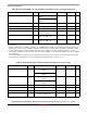
Table 28. Single-voltage 1.8 V GPIO DC parameters
Parameter Symbol Test Conditions
1
Min Max Units
High-level output voltage
2
V
OH
I
OH
= -0.1mA
DSE = 000 or 001
OVDD × 0.8 — V
I
OH
= -2mA
DSE = 010 or 011
I
OH
= -4mA
DSE = 100 to 110
Low-level output voltage
2
V
OL
I
OL
= 0.1mA
DSE = 000 or 001
—OVDD× 0.2 V
I
OL
= 2mA
DSE = 010 or 011
I
OL
= 4mA
DSE = 100 to 110
High-Level input voltage
2,3
V
IH
—0.65× OVDD OVDD V
Low-Level input voltage
2,3
V
IL
— 0 0.35 × OVDD V
Input Hysteresis V
HYS
—100—mV
Pull-up resistance R
PU
Vin=0V (Pullup Resistor)
PUN = "L", PDN = "H"
20 90 kΩ
Pull-down resistance R
down
Vin=OVDD( Pulldown Resistor)
PUN = "H", PDN = "L"
20 90 kΩ
Table 27. Dual-voltage GPIO 3.3 V DC parameters
1
(IO PSW is set to 3.3 V range) (continued)
Parameter Symbol Test Conditions
2
Min Max Units