
Datasheet


Electrical characteristics
i.MX 8QuadXPlus and 8DualXPlus Automotive and Infotainment Applications Processors, Rev. 0, 11/2018
PRELIMINARY NXP Semiconductors32
CAUTION
The internal oscillator provides an estimated frequency accuracy of ±5%,
subject to silicon validation, and is affected by process, voltage and
temperature variations. NXP strongly recommends using an external crystal
to implement an oscillator. If the internal oscillator is used instead, careful
consideration must be given to the timing implications on all of the SoC
modules dependent on this clock. The OSC32K runs from
VDD_SNVS_1p8_CAP, which is regulated from VDD_SNVS. The target
battery is 2.8V ~ 4.2V for VDD_SNVS and the regulated output is ~1.75V.
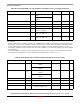
Table 24. OSC32K Main Characteristics
Parameter Min Typ Max Comments
Fosc — 32.768 kHz — This frequency is nominal and determined mainly by
the crystal selected. 32.0 KHz is also supported.
Current
consumption
— • xtal oscillator mode: 5 μA
• 32K internal oscillator mode: 10 μA
— These values are for typical process and room
temperature. Values will be updated after silicon
characterization.
Bias resistor — 200 MΩ — This the integrated bias resistor that sets the amplifier
into a high gain state. Any leakage through the ESD
network, external board leakage, or even a scope
probe that is significant relative to this value will
debias the amplifier. The debiasing will result in low
gain, and will impact the circuit's ability to start up and
maintain oscillations.
Target Crystal Properties
Cload — 10 pF — Usually crystals can be purchased tuned for different
Cloads. This Cload value is typically 1/2 of the
capacitances realized on the PCB on either side of
the quartz. A higher Cload will decrease oscillation
margin, but increases current oscillating through the
crystal.
ESR — 50 kΩ 100 kΩ Equivalent series resistance of the crystal. Choosing
a crystal with a higher value will decrease the
oscillating margin.
Table 25. External input clock for OSC32K
Min Typ Max Unit Notes
Frequency — 32.768 or 32 — kHz —
V
PP
RTC_XTALI 700 — VDD_SNVS_1P8_CAP mV
1,2,3
1
The external clock is fed into the chip from the RTC_XTALI pin; the RTC_XTALO pin should be left floating.
2
The parameter specified here is a peak-to-peak value and VI
H/
V
IL
specifications do not apply.
3
The voltage applied on RTC_XTALI must be within the range of VSS to VDD_SNVS_1P8_CAP.
Rise/fall time — — — ns
4