
Datasheet


Electrical characteristics
i.MX 8QuadXPlus and 8DualXPlus Automotive and Infotainment Applications Processors, Rev. 0, 11/2018
PRELIMINARYNXP Semiconductors 21
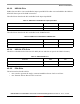
The typical values shown in Table 7 are required for use with NXP board support packages (BSPs) to
ensure precise time keeping and USB operations.
4.1.5 Maximum Supply Currents
2
The required frequency stability of this clock source is application dependent. For recommendations, see the Hardware
Development Guide.
3
Recommended nominal frequency 32.768 kHz.
4
Fundamental frequency crystal with internal oscillator amplifier.
5
If using an external clock instead of the internal clock source, an HCSL-compatible clock is required.
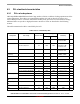
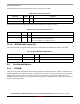
Table 8. Maximum supply currents
Symbol Value Unit Comments
VDD_A35
1
2500 mA Value based on max current delivered by PMIC
VDD_GPU
1
2500 mA Value based on max current delivered by PMIC
VDD_MAIN 5000 mA Value based on max current delivered by PMIC
VDD_DDR_VDDQ 1200 mA Does not comprehend IO of memory
VDD_DDR_PLL_1P8 20 mA
VDD_ANA0_1P8 200 mA
VDD_ANA1_1P8 200 mA
VDD_MIPI_1P0 100 mA
VDD_MIPI_1P8 115 mA
VDD_ADC_DIG_1P8 18 mA
VDD_CAN_UART_1P8_3P3 30 mA
VDD_CSI_1P8_3P3 12 mA
VDD_EMMC0_1P8_3P3 30 mA
VDD_EMMC0_VSELECT_1P8_3P3 30 mA
VDD_ENET_MDIO_1P8_3P3 15 mA
VDD_ENET0_1P8_2P5_3P3 30 mA
VDD_ENET0_VSELECT_1P8_2P5_3
P3
30 mA
VDD_ESAI_SPDIF_1P8_2P5_3P3 39 mA
VDD_MIPI_CSI_DIG_1P8 15 mA
VDD_MIPI_DSI_DIG_1P8_3P3 24 mA
VDD_PCIE_DIG_1P8_3P3 9 mA
VDD_QSPI0A_1P8_3P3 40 mA
VDD_QSPI0B_1P8_3P3 40 mA