
Datasheet


Electrical characteristics
i.MX 8QuadXPlus and 8DualXPlus Automotive and Infotainment Applications Processors, Rev. 0, 11/2018
PRELIMINARY NXP Semiconductors16
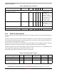
4.1.2 Thermal resistance
4.1.2.1 FCPBGA package thermal resistance
This table provides the FCPBGA package thermal resistance data.
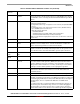
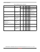
I/O Voltage for USB Drivers USB_OTG1_DP/USB_OTG1_DN -0.3 3.63 V
USB_OTG2_DP/USB_OTG2_DN
I/O Voltage for ADC ADC_IN
x
-0.1 2.1 V
Vin/Vout input/output voltage range (GPIO
Type Pi n s )
Vin/Vout -0.3 OVDD+0.3
1
V
Vin/Vout input/output voltage range (DDR
pins)
Vin/Vout -0.3 OVDD+0.4
1,2
V
ESD immunity (HBM). All pins except PCIe
differential pairs, HDMI-RX, HDMI-TX, and
USB3 (including OTG2) interfaces.
Vesd_HBMX —
2000 V
ESD immunity (CDM). All pins except PCIe
differential pairs, HDMI-RX, HDMI-TX, and
USB3 (including OTG2) interfaces.
Vesd_CDM — 500 V
ESD immunity (HBM) for PCIe differential
pairs, HDMI-RX, HDMI-TX, and USB3
(including OTG2) interfaces.
Vesd_HBMX —
1000 V
ESD immunity (CDM) for PCIe differential
pairs, HDMI-RX, HDMI-TX, and USB3
(including OTG2) interfaces.
Vesd_CDM —
250 V
Storage temperature range Tstorage -40 150 °C
1
OVDD is the I/O supply voltage.
2
The absolute maximum voltage includes an allowance for 400 mV of overshoot on the I/O pins. Per JEDEC standard the allowed
signal overshoot must be derated if NVCC_DRAM exceeds 1.575 V.
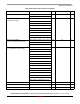
Table 5. FCPBGA package thermal resistance data
1
Thermal Parameter Test Conditions Symbol
21x21 mm
package
17x17 mm
package
Unit
Junction to Ambient
2
Single-layer board (1s); natural
convection
3
R
θJA
27.7 31.8 °C/W
Four-layer board (2s2p); natural
convection
2
R
θJA
15.2 15.8 °C/W
Table 4. Absolute maximum ratings (continued)
Parameter Description Symbol Min Max Units