
Datasheet


Electrical characteristics
i.MX 8QuadXPlus and 8DualXPlus Automotive and Infotainment Applications Processors, Rev. 0, 11/2018
PRELIMINARYNXP Semiconductors 105
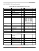
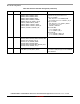
The following table shows the ADC electrical specifications for 1V≤VREFH<VDD_ADC_1P8.
Table 107. ADC electrical specifications (1V≤VREFH<VDD_ADC_1P8)
Symbol Description Min Typ
1
1
Typical values assume VDD_ANA_18 = 1.8 V, Temp = 25 °C, fACLK = Max, unless otherwise stated. Typical values are for
reference only and are not tested in production.
Max Unit Notes
V
ADIN
Input Voltage VREFL — VREFH V —
C
ADIN
Input capacitance — 4.5 — pF —
R
ADIN
Input Resistance — 500 — Ω —
R
AS
Analog Source Resistance — — 5 kΩ
2
2
This resistance is external to the input pad. To achieve the best results, the analog source resistance must be kept as low as
possible. The results in this data sheet were derived from a system that had < 15 Ω analog source resistance. The RAS/CAS
(analog source capacitance) time constant should be kept to < 1 ns.
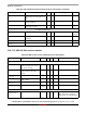
f
ADCK
ADC Conversion Clock Frequency — 24 — MHz —
C
sample
Sample cycles 3.5 — 131.5 —
3
3
See Figure 57.
C
compare
Fixed compare cycles — 17.5 — cycles —
C
conversion
Conversion cycles C
conversion =
C
sample +
C
compare
cycles —
DNL Differential Non-Linearity — ± 0.6 -0.5 to +1 LSB
4
4
ADC conversion clock at max frequency and using linear histogram.
INL Integral Non-Linearity — ± 0.9 ±1 LSB
4
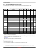
ENOB Effective Number of Bits — — — —
5,6
5
Input data used for test was 1 kHz sine wave.
6
Measured at VREFH = 1 V and pwrsel = 2.
Avg = 1 9.5 9.7 — Bits
Avg = 2 9.9 10.1 — Bits
Avg = 16 10.8 11 — Bits
SINAD Signal to Noise plus Distortion SINAD=6.02 x ENOB + 1.76 dB —
E
G
Gain error — 0.29 — %FSV
7
7
Error measured at fullscale at 1.0 V.
E
O
Offset error — 0.01 — %FSV
8
8
Error measured at zero scale at 0 V.
I
VDDA18
Supply Current — 480 — μA
9
9
Power Configuration Select, PWRSEL, is set to 10 binary which is the highest power setting.
I
in,ext,leak
External Channel Leakage Current — 30 500 nA —
E
IL
Input leakage error RAS * I
in
mV —