
Datasheet


Electrical characteristics
i.MX 8QuadXPlus and 8DualXPlus Automotive and Infotainment Applications Processors, Rev. 0, 11/2018
PRELIMINARYNXP Semiconductors 103
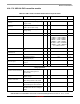
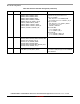
Table 105. PLL module electrical specifications
Parameter Symbol Description Min Typ Max Units
Input Reference Clock
REF CLK
Frequency
REF CLK — 19.2 19.2/24/25/26/38.4 38.4 MHz
REF CLK Duty
Cycle
——47—53MHz
REF CLK
Frequency
REF CLK — 40 40/48/50/52/100 100 MHz
REF CLK RJ
Tolerance
— Integrated jitter from 10 kHz to 16 MHz
after applying appropriate PLL ref clock
transfer function and the protocol JTF
——0.5ps
REF CLK Duty
Cycle
——37—63%
Divided Reference
Frequency
— — 19.2 — 38.4 MHz
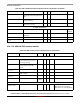
Dividers
Input division IPDIV<7:0> — 1 — 255 Counts
Feedback division pll_fbdiv_high<9:0> — 2 — 1025 Counts
pll_fbdiv_low<9:0> — 2 — 1025 Counts
Feedback fractional
division range
——>-2—<2Counts
Number of
fractional bits
— This includes one bit for sign — 27 — Bits
VCO
Clock frequency — Output full rate clocks — 5000 — MHz
VCO frequency — VCO oscillation frequency — 5000 — MHz
Output clock
frequency tolerance
— This includes SSC deviation -5300 — 300 ppm
SSC modulation
rate
— As applicable for USB3.0 30 — 33 kHz
Output clock RJ
sigma for TX
— After application of TX jitter transfer
function
— — 2.42 ps
Output clock RJ
sigma for RX
— After application of RX jitter transfer
function
— — 1.40 ps