
User guide


MOTOROLA DSPAUDIOEVM Evaluation Board Users Manual 13
This document contains information on a new product. Specifications and information herein are subject to change without notice.
3.3 Memory
The daughterboard includes three 128Kx8 SRAM (one 128Kx8 SRAM for the 56364 daughterboard). There
is also a 512Kx8 FLASH device resident on the board. From factory the FLASH is programmed with an
audio passthru code to allow simple verification of initial board operations. See Section 1.8 Running the
Passthru Code for an explanation of running the passthru code.
3.4 JP11 - Clock Selection
Jumper bank JP11 allows for the following clocking modes:
OSC – Clock DSP from canned oscillator at U7 (not Populated)
XTAL – Clock DSP from 24.576MHz crystal at X1 (default mode)
EXT – Clock DSP from motherboard 24.576MHz clock source
Only one of the JP11 options should be populated at the same time.
3.5 Daughterboard Audio I / O and Clock Control Header
3.5.1 TIO0 – Timmer Port
This is connected directly to the TIO0 pin on the DSP.
3.5.2 JP1 - Synchronous/Asynchronous Clock Control
This jumper set controls whether or not the DSP is in synchronous or asynchronous mode. Position B allows
the DSP GPIO (pin PB9) to choose the mode. Position C forces the mode to be asynchronous, and no
jumper forces synchronous mode. In synchronous mode FST is connected to FSR, and SCKT is connected
to SCKR on the ESAI port of the DSP.
3.5.3 JP2 – Single/Double Speed Clocking Control
This jumper set controls whether or not the motherboard is in single or double speed mode. Position D
forces the motherboard into double speed mode. Position E allows the DSP GPIO pin PB11 to control the
mode (e.g., through a PPP), and no jumper forces single speed mode. An example of this signal’s use is for
decoding of DTS 96/24 content. In this mode, it is required to update the masterclock ration expectation in
the D/A converters and S/PDIF transmitters because the DTS 96/24 decoder doubles the audio sample rate
as part of the decoding process.
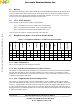
Table 3.3 Daughterboard Audio I / O and Clock Control Header
TIO0
Sync/Async
Sng/Dbl
FST_1
SCKT_1
FSR_1
SCKR_1
DSP MUTE
INTO
SDO5/SDI0
SDO4/SDI1
* * * * * * * * * * * * * * * * *
* * * * * * * * * * * * * * * * *
A B C D E F G H I J K L M N O P Q
TI0 JP1 JP2 JP3 JP4 JP5 JP6 JP7 JP8 JP9 JP10
Frees
cale Semiconductor,
I
Freescale Semiconductor, Inc.
For More Information On This Product,
Go to: www.freescale.com
nc...