
User guide

8 DSPAUDIOEVM Evaluation Board Users Manual MOTOROLA
This document contains information on a new product. Specifications and information herein are subject to change without notice.
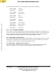
2.3.2 P2 — OnCE Header
The P2 OnCE header is for connection of an external OnCE/JTAG debugger tool to the OnCE/JTAG port of the
DSP on the daughterboard. Further explanation of the OnCE/JTAG signal definition can be found in the DSP
users manuals. The P2 OnCE header is for connection of an external OnCE/JTAG debugger tool to the OnCE/
JTAG port of the DSP on the daughterboard. Further explanation of the OnCE/JTAG signal definition can be found
in the DSP users manuals. Note that when using an external OnCE/JTAG debugger tool, the JP9 JTAG jumper
should be in the "OnCE" position.
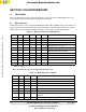
2.3.3 P3 — ANALOG I/O
The Analog I/O header allows for analog access to input signals before the A/D (AIN1) op-amp stage and
the output signals after the D/A (AO1-6) op-amp stage. This section is provided for ease of analog
measurement and analog I/O connector relocation.
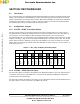
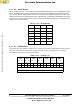
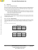
Table 2.7 P2 — OnCE Header
TDI(1) * * GND
TDO * * GND
TCK * * GND
N/C * KEY
RESET * * TMS
VDD * * N/C
N/C * * N/C
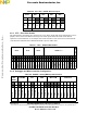
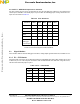
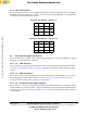
Table 2.8 P3 — Analog I / O
AO6 AO5 AO4 AO3 AO2 AO1 AIN1
R L R L R L R L R L R L R L
* * * * * * * * * * * * * *
* * * * * * * * * * * * * *
GND
P3
Frees
cale Semiconductor,
I
Freescale Semiconductor, Inc.
For More Information On This Product,
Go to: www.freescale.com
nc...