
Datasheet


1999 Apr 26 2
NXP Semiconductors Product data sheet
PNP general purpose double transistor BC857BS
FEATURES
• Low collector capacitance
• Low collector-emitter saturation voltage
• Closely matched current gain
• Reduces number of components and boardspace
• No mutual interference between the transistors.
APPLICATIONS
• General purpose switching and amplification.
DESCRIPTION
PNP double transistor in an SC-88; SOT363 plastic
package. NPN
complement: BC847BS.
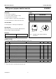
MARKING
PINNING
TYPE NUMBER MARKING CODE
BC857BS 3Ft
PIN DESCRIPTION
1, 4 emitter TR1; TR2
2, 5 base TR1; TR2
6, 3 collector TR1; TR2
Fig.1 Simplified outline (SC-88; SOT363)
and symbol.
handbook, halfpage
132
4
56
Top view
MAM339
132
TR1
TR2
6
4
5
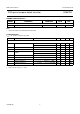
LIMITING VALUES
In accordance with the Absolute Maximum Rating System (IEC 134).
Note
1. Device mounted on an FR4 printed-circuit board.
SYMBOL PARAMETER CONDITIONS MIN. MAX. UNIT
Per transistor
V
CBO
collector-base voltage open emitter − −50 V
V
CEO
collector-emitter voltage open base − −45 V
V
EBO
emitter-base voltage open collector − −5 V
I
C
collector current (DC) − −100 mA
I
CM
peak collector current − −200 mA
I
BM
peak base current − −200 mA
P
tot
total power dissipation T
amb
≤ 25 °C − 200 mW
T
stg
storage temperature −65 +150 °C
T
j
junction temperature − 150 °C
T
amb
operating ambient temperature −65 +150 °C
Per device
P
tot
total power dissipation Tamb ≤ 25 °C; note 1 − 300 mW