
Datasheet

NXP Semiconductors
88W8977
2.4 GHz/5 GHz Dual-band 1x1 Wi-Fi 4
®
and Bluetooth
®
5 Combo SoC
88W8977 All information provided in this document is subject to legal disclaimers. © NXP B.V. 2020. All rights reserved.
Product short data sheet Rev. 1 — 13 July 2020
66 / 81
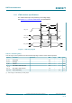
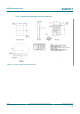
9.3 Package marking
9.3.1 68-pin QFN package marking
88W8977-NMV2
Lot Number
YYWW xx#
Country of Origin
Country of Origin
(Contained in the mold ID or
marked as the last line on the
package)
Pin 1 Location
Note: The above drawing is not drawn to scale. The location of markings is approximate.
Date code, Die revision, Assembly Plant
YYWW = Date Code
(YY = Year, WW = Work Week)
xx = Revision number
# = Assembly Plant Code
Part Number, Package Code,
Environmental Code
xxx = package code
E005
Temperature/Band code
E005 = Extended temperature
I005 = Industrial temperature
Figure 22. 68-pin QFN package marking and pin 1 location
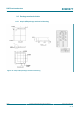
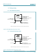
9.3.2 74-bump eWLP package marking
W8977EAD
Lot Number
YYWW xx#
Country of Origin E005
Country of Origin
(Contained in the mold ID or
marked as the last line on the
package)
Pin 1 Location
Note: The above drawing is not drawn to scale. The location of markings is approximate.
Date code, Die revision, Assembly Plant
YYWW = Date Code
(YY = Year, WW = Work Week)
xx = Revision number
# = Assembly Plant Code
Part Number, Package Code,
Environmental Code
xxx = package code
Temperature/Band code
E005 = Extended temperature (2.4/5 GHz)
None = Extended temperature (2.4 GHz)
Figure 23. 74-bump eWLP package marking and pin 1 location