
Datasheet

NXP Semiconductors
88W8977
2.4 GHz/5 GHz Dual-band 1x1 Wi-Fi 4
®
and Bluetooth
®
5 Combo SoC
88W8977 All information provided in this document is subject to legal disclaimers. © NXP B.V. 2020. All rights reserved.
Product short data sheet Rev. 1 — 13 July 2020
61 / 81
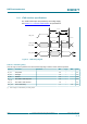
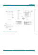
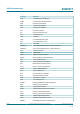
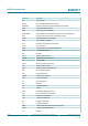
8.11 JTAG interface specifications
The JTAG interface pins are powered by VIO voltage supply.
See Section 8.1.1 "VIO DC characteristics" for specifications.
JTAG_TCK
JTAG_TDO
T
DLY_TDO
JTAG_TMS
JTAG_TDI
T
H_TCK
T
P_TCK
T
L_TCK
T
SU_TDI
T
HD_TDI
Figure 19. JTAG timing diagram
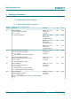
Table 52. JTAG timing data
[1]
Over full range of values specified in the Recommended Operating Conditions unless otherwise specified.
Symbol Parameter Condition Min Typ Max Unit
T
P_TCK
TCK period -- 40 -- -- ns
T
H_TCK
TCK high -- 12 -- -- ns
T
L_TCK
TCK low -- 12 -- -- ns
T
SU_TDI
TDI, TMS to TCK setup time -- 10 -- -- ns
T
HD_TDI
TDI, TMS to TCK hold time -- 10 -- -- ns
T
DLY_TDO
TCK to TDO delay -- 0 -- 15 ns
[1] Does not apply to JTAG enabled by the JTAG_TMS pin.