
Datasheet


NXP Semiconductors
88W8977
2.4 GHz/5 GHz Dual-band 1x1 Wi-Fi 4
®
and Bluetooth
®
5 Combo SoC
88W8977 All information provided in this document is subject to legal disclaimers. © NXP B.V. 2020. All rights reserved.
Product short data sheet Rev. 1 — 13 July 2020
60 / 81
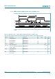
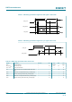
8.10.2 Crystal
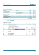
Table 50. Crystal specifications
Parameter Condition Typical Unit
Fundamental frequencies -- 26 MHz
Over operating temperature < ±10 ppmFrequency tolerance
Over process at 25ºC < ±10 ppm
SMD and AT cut height -- <1.2 mm
Load Capacitance -- 5 pF
Maximum series resistance -- 45 Ω
Resonance mode -- A1,
Fundamental
--
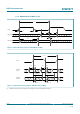
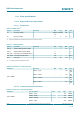
8.10.3 Sleep clock
Table 51. External sleep clock timing
Limited to within 10°C variance.
Symbol Parameter Min Typ Max Unit
CLK Clock frequency range/accuracy
• CMOS input clock signal type
• ±250 ppm (initial, aging, temperature)
-- 32.768 -- kHz
V
IH
0.7*VIO -- VIO+0.4 V
V
IL
Input levels, where VIO = 1.8, 2.5, 3.3V
For VIH, VIL, see Section Section 8.1.1 "VIO DC characteristics".
-0.4 -- 0.3*VIO V
PN Phase noise requirement (at 100 kHz) -- -125 -- dBc
/Hz
Jc Cycle jitter -- 1.5 -- ns
(RMS)
SR Slew rate limit (10-90%) -- -- 100 ns
DC Duty cycle tolerance 20 -- 80 %