
Datasheet


NXP Semiconductors
88W8977
2.4 GHz/5 GHz Dual-band 1x1 Wi-Fi 4
®
and Bluetooth
®
5 Combo SoC
88W8977 All information provided in this document is subject to legal disclaimers. © NXP B.V. 2020. All rights reserved.
Product short data sheet Rev. 1 — 13 July 2020
59 / 81
8.10 Clock specifications
8.10.1 Single-ended clock input modes
8.10.1.1 2.4 GHz mode
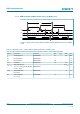
Table 46. CMOS mode
[1]
Symbol Parameter Condition Min Typ Max Unit
V
IH
Input high voltage -- AVDD18
- 0.5
AVDD18 1.98 V
V
IL
Input low voltage -- 0 0 0.4 V
[1] Typical input capacitance is approximately 2 pF and input resistance is >20 kΩ.
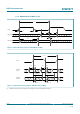
Table 47. Low-Swing Mode
[1]
Symbol Parameter Condition Min Typ Max Unit
VLS_IH Single-ended high-level voltage -- -- -- 1.8 V
VLS_IL Single-ended low-level voltage -- 0 -- -- V
VLS_Amp Low-swing clock amplitude (pk-pk) -- 0.5 -- -- V
VLS_Slope Low-swing mid-point slope -- 100 -- -- MV/s
Duty Duty cycle -- 45 50 55 %
[1] AC-coupling capacitor is integrated into the SoC.
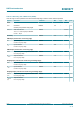
Table 48. Phase Noise—2.4 GHz operation
Parameter Condition Min Typ Max Unit
Offset = 1 kHz -- -- -126 dBc
/Hz
Offset = 10 kHz -- -- -137 dBc
/Hz
Offset = 100 kHz -- -- -145 dBc
/Hz
Fref = 26 MHz
Offset > 1 MHz -- -- -145 dBc
/Hz
8.10.1.2 2.4 GHz and 5 GHz dual-band mode
Table 49. Phase noise—Dual-band operation
Parameter Test Conditions Min Typ Max Unit
Offset = 1 kHz -- -- -130 dBc/Hz
Offset = 10 kHz -- -- -150 dBc/Hz
Offset = 100 kHz -- -- -156 dBc/Hz
Fref = 26 MHz
Offset > 1 MHz -- -- -156 dBc/Hz