
Datasheet


NXP Semiconductors
88W8977
2.4 GHz/5 GHz Dual-band 1x1 Wi-Fi 4
®
and Bluetooth
®
5 Combo SoC
88W8977 All information provided in this document is subject to legal disclaimers. © NXP B.V. 2020. All rights reserved.
Product short data sheet Rev. 1 — 13 July 2020
58 / 81
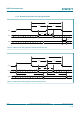
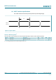
Table 43. PCM timing specification diagram for data signals—Slave mode
PCM_CLK
PCM_DOUT
PCM_DIN
T
BCLK
T
DIHO
T
DISU
T
DO
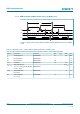
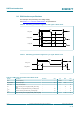
Table 44. PCM timing specification diagram for sync signal—Slave mode
PCM_CLK
PCM_SYNC
T
BCLK
T
BFHO
T
BF
T
BFSU
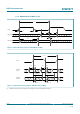
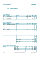
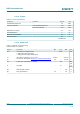
Table 45. PCM timing specification data—Slave mode
Symbol Parameter Condition Min Typ Max Unit
F
BCLK
Bit clock frequency -- -- 2/2.048 -- MHz
Duty Cycle
BCLK
Bit clock duty cycle -- 0.4 0.5 0.6 --
T
BCLK rise/fall
PCM_CLK rise/fall time -- -- 3 -- ns
T
DO
Delay from PCM_CLK rising edge to PCM_DOUT rising
edge
-- -- -- 30 ns
T
DISU
Setup time for PCM_DIN before PCM_CLK falling edge -- 15 -- -- ns
T
DIHO
Hold time for PCM_DIN after PCM_CLK falling edge -- 10 -- -- ns
T
BFSU
Setup time for PCM_SYNC before PCM_CLK falling edge -- 15 -- -- ns
T
BFHO
Hold time for PCM_SYNC after PCM_CLK falling edge -- 10 -- -- ns