
Datasheet


NXP Semiconductors
88W8977
2.4 GHz/5 GHz Dual-band 1x1 Wi-Fi 4
®
and Bluetooth
®
5 Combo SoC
88W8977 All information provided in this document is subject to legal disclaimers. © NXP B.V. 2020. All rights reserved.
Product short data sheet Rev. 1 — 13 July 2020
57 / 81
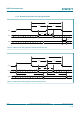
8.9 PCM interface specifications
The PCM pins are powered by VIO voltage supply.
See Section 8.1.1 "VIO DC characteristics" for specifications.
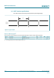
Table 40. PCM timing specification diagram for data signals—Master mode
PCM_CLK
PCM_DOUT
PCM_DIN
T
BCLK
T
DIHO
T
DISU
T
DO
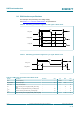
Table 41. PCM timing specification diagram for sync signal—Master mode
PCM_CLK
PCM_SYNC
T
BCLK
T
BCLK
T
BF
T
BF
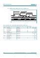
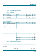
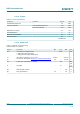
Table 42. PCM timing specification data—Master mode
Symbol Parameter Condition Min Typ Max Unit
F
BCLK
Bit clock frequency -- -- 2/2.048 -- MHz
Duty Cycle
BCLK
Bit clock duty cycle -- 0.4 0.5 0.6 --
T
BCLK rise/fall
PCM_CLK rise/fall time -- -- 3 -- ns
T
DO
Delay from PCM_CLK rising edge to PCM_DOUT rising
edge
-- -- -- 15 ns
T
DISU
Setup time for PCM_DIN before PCM_CLK falling edge -- 20 -- -- ns
T
DIHO
Hold time for PCM_DIN after PCM_CLK falling edge -- 15 -- -- ns
T
BF
Delay from PCM_CLK rising edge to PCM_SYNC rising edge -- -- -- 15 ns