
Datasheet


NXP Semiconductors
88W8977
2.4 GHz/5 GHz Dual-band 1x1 Wi-Fi 4
®
and Bluetooth
®
5 Combo SoC
88W8977 All information provided in this document is subject to legal disclaimers. © NXP B.V. 2020. All rights reserved.
Product short data sheet Rev. 1 — 13 July 2020
55 / 81
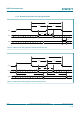
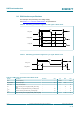
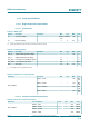
Table 38. SDIO timing data—DDR50 mode (50 MHz)
Over full range of values specified in the Recommended Operating Conditions unless otherwise specified.
Symbol Parameter Condition Min Typ Max Unit
Clock
T
CLK
Clock time
50 MHz (max) between rising edges
DDR50 20 -- -- ns
T
CR
, T
CF
Rise time, fall time
T
CR
, T
CF
< 4.00 ns (max) at 50 MHz
C
CARD
= 10 pF
DDR50 -- -- 0.2*T
CLK
ns
Clock Duty -- DDR50 45 -- 55 %
CMD Input (referenced to clock rising edge)
T
IS
Input setup time
C
CARD
≤ 10 pF (1 card)
DDR50 6 -- -- ns
T
IH
Input hold time
C
CARD
≤ 10 pF (1 card)
DDR50 0.8 -- -- ns
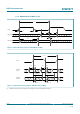
CMD Output (referenced to clock rising edge)
T
ODLY
Output delay time during data transfer mode
C
L
≤ 30 pF (1 card)
DDR50 -- -- 13.7 ns
T
OHLD
Output hold time
C
L
≥ 15 pF (1 card)
DDR50 1.5 -- -- ns
DAT[3:0] Input (referenced to clock rising and falling edges)
T
IS2x
Input setup time
C
CARD
≤ 10 pF (1 card)
DDR50 3 -- -- ns
T
IH2x
Input hold time
C
CARD
≤ 10 pF (1 card)
DDR50 0.8 -- -- ns
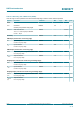
DAT[3:0] Output (referenced to clock rising and falling edges)
T
ODLY2x
(max)
Output delay time during data transfer mode
C
L
≤ 25 pF (1 card)
DDR50 -- -- 7.0 ns
T
ODLY2x
(min)
Output hold time
C
L
≥ 15 pF (1 card)
DDR50 1.5 -- -- ns