
Datasheet


NXP Semiconductors
88W8977
2.4 GHz/5 GHz Dual-band 1x1 Wi-Fi 4
®
and Bluetooth
®
5 Combo SoC
88W8977 All information provided in this document is subject to legal disclaimers. © NXP B.V. 2020. All rights reserved.
Product short data sheet Rev. 1 — 13 July 2020
54 / 81
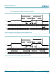
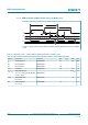
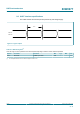
8.7.4 DDR50 Mode (50 MHz) (1.8V)
CMD input
Clock
CMD output
T
ODLY
T
IH
T
IS
T
CLK
T
CR
T
CF
T
OHLD
Figure 16. SDIO CMD timing diagram—DDR50 Mode (50 MHz)
DAT[3:0]
Input
Clock
DAT[3:0]
Output
T
CLK
T
IH2x
T
IS2x
T
IH2x
T
IS2x
T
ODLY2x (max)
T
ODLY2x (max)
T
ODLY2x (min)
T
ODLY2x (min)
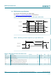
Figure 17. SDIO DAT[3:0] timing diagram—DDR50 mode
[1]
(50 MHz)
[1] In DDR50 mode, DAT[3:0] lines are sampled on both edges of the clock (not applicable for CMD line).