
Datasheet


NXP Semiconductors
88W8977
2.4 GHz/5 GHz Dual-band 1x1 Wi-Fi 4
®
and Bluetooth
®
5 Combo SoC
88W8977 All information provided in this document is subject to legal disclaimers. © NXP B.V. 2020. All rights reserved.
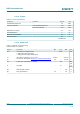
Product short data sheet Rev. 1 — 13 July 2020
53 / 81
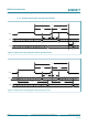
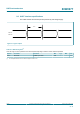
8.7.3 SDR12, SDR25, SDR50 modes (up to 100 MHz) (1.8V)
f
PP
Input
Clock
Output
T
ODLY
T
IH
T
IS
T
OH
T
CLK
T
CR
T
CF
Figure 15. SDIO protocol timing diagram—SDR12, SDR25, SDR50 modes (up to 100 MHz)
(1.8V)
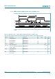
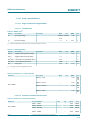
Table 37. SDIO timing data——SDR12, SDR25, SDR50 modes (up to 100 MHz) (1.8V)
Over full range of values specified in the Recommended Operating Conditions unless otherwise specified.
Symbol Parameter Condition Min Typ Max Unit
f
PP
Clock frequency SDR12/25/50 25 -- 100 MHz
T
IS
Input setup time SDR12/25/50 3 -- -- ns
T
IH
Input hold time SDR12/25/50 0.8 -- -- ns
T
CLK
Clock time SDR12/25/50 10 -- 40 ns
T
CR
, T
CF
Rise time, fall time
T
CR
, T
CF
< 2 ns (max) at 100 MHz
C
CARD
= 10 pF
SDR12/25/50
-- -- 0.2*T
CLK
ns
T
ODLY
Output delay time
C
L
≤ 30 pF
SDR12/25/50 -- -- 7.5 ns
T
OH
Output hold time
C
L
= 15 pF
SDR12/25/50 1.5 -- -- ns