
Datasheet


NXP Semiconductors
88W8977
2.4 GHz/5 GHz Dual-band 1x1 Wi-Fi 4
®
and Bluetooth
®
5 Combo SoC
88W8977 All information provided in this document is subject to legal disclaimers. © NXP B.V. 2020. All rights reserved.
Product short data sheet Rev. 1 — 13 July 2020
26 / 81
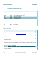
5 Power information
The table in Section 4.4.12 "Power supply and ground pins " shows the required voltage
levels for each rail and PDn input signal.
5.1 Leakage optimization
For applications not using Wi-Fi and Bluetooth, the device can be put into a low-leakage
mode of operation. Methods include:
• Using the power-down (PDn) pin
The power-down state provides the lowest leakage mode of operation. Assert PDn low
to enter power-down. If the firmware is not downloaded, the device must be kept in
power-down mode to reduce leakage.
• All rails powered off
Alternatively, all power rails can be powered off. In this case, the state of PDn pin is
irrelevant.
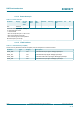
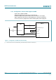
5.2 Power-up
The 88W8977 VCORE is supplied through either an external PMIC or the internal LDO.
In both cases, the PDn pin of the 88W8977 is tied to 1.8V.
The power configurations include:
• Section 5.2.1 "Configuration—PMIC supplies VCORE"
• Section 5.2.2 "Configuration—Internal LDO supplies VCORE"
In either configuration, the ramp-up is controlled by the Host using the PMIC_EN pin.
• PMIC_EN represents the input enable pin (EN) of the power regulator.
• PMIC_EN ramps up from Host 3.3V
• PMIC_EN ramps up from Host GPIO pin
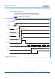
Section 5.2.3 "Power-up sequence" shows the power-up sequence for both
configurations.