
Datasheet


NXP Semiconductors
88W8977
2.4 GHz/5 GHz Dual-band 1x1 Wi-Fi 4
®
and Bluetooth
®
5 Combo SoC
88W8977 All information provided in this document is subject to legal disclaimers. © NXP B.V. 2020. All rights reserved.
Product short data sheet Rev. 1 — 13 July 2020
24 / 81
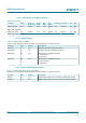
4.4.14 Power-down pin
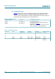
Table 14. Power-down pin
Pin Name Supply No Pad
Power
State
Reset
State
HW
State
PD State PD Prog Internal PU/
PD
PU PD
PDn AVDD18 -- -- -- -- -- -- -- --
Full Power-Down (input) (active low)
0 = full power-down mode
1 = normal mode
• PDn can accept an input of 1.8V to 4.5V
• PDn may be driven by the host
• PDn must be high for normal operation
No internal pull-up on this pin.
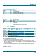
4.4.15 JTAG interface
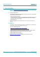
Table 15. JTAG interface pins (MFP)
NOTE: Pins may be Multi-Functional Pins (MFP). See pin descriptions for functional modes.
Pin Name Type Supply Description
JTAG_TDO O VIO JTAG test data output signal. GPIO[3] input/output
JTAG_TDI I VIO JTAG test data input signal. GPIO[2] input/output
JTAG_TMS I VIO JTAG test mode select input signal. GPIO[15] input/output
JTAG_TCK I VIO JTAG test clock input signal. GPIO[14] input/output