
Datasheet


NXP Semiconductors
88W8977
2.4 GHz/5 GHz Dual-band 1x1 Wi-Fi 4
®
and Bluetooth
®
5 Combo SoC
88W8977 All information provided in this document is subject to legal disclaimers. © NXP B.V. 2020. All rights reserved.
Product short data sheet Rev. 1 — 13 July 2020
23 / 81
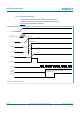
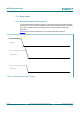
4.4.12 Power supply and ground pins
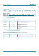
Table 12. Power supply and ground pins
Pin Name Type Description
VCORE Power 1.05V Core Power Supply
VIO Power 1.8V/2.5V/3.3V Digital I/O Power Supply
VIO_SD Power 1.8V/3.3V Digital I/O SDIO Power Supply
VIO_RF Power 1.8V/3.3V Analog I/O RF Power Supply
AVDD18 Power 1.8V Analog Power Supply
VPA Power 2.2V Analog Power Supply
LDO_VIN Power LDO Voltage Input (1.8V)
LDO_VOUT Power LDO Voltage Output
AVSS Ground Ground
VSS Ground Ground
NC NC No Connected
DNC DNC Do Not Connect
Do not connect these pins. Leave these pins floating.
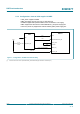
4.4.13 Clock interface
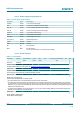
Table 13. Clock interface
Pin Name Supply No Pad Power
State
Reset
State
HW
State
PD PD Prog Internal PU/
PD
PU PD
XTAL_IN AVDD18 -- -- -- -- -- -- -- --
Crystal / Crystal Oscillator / System Clock Input
Accepts 26 MHz reference clock signal. See Section 8.10 "Clock specifications".
XTAL_OUT AVDD18 -- -- -- -- -- -- -- --
Crystal / Crystal Oscillator Output
Connect this pin to ground when an external oscillator is used.
SLP_CLK_IN VIO tristate input input tristate no nominal PU yes yes
Sleep Clock Input (optional)
Used for Wi-Fi and Bluetooth low-power modes.
• An external sleep clock is recommended for minimal current consumption.
• If no sleep clock input is provided, an internal sleep clock (derived from reference clock) will be used. This will cause
an approximate ~50 uA current increase on the 3.3V rail, since the reference clock cannot be shut down during device
sleep. If SLP_CLK_IN is not connected, the internal circuit will detect no signal, and firmware will initialize the sleep clock
based on the reference clock.
• To reduce further leakage, do not ground the SLP_CLK_IN pin / keep it floating (DNC) for cases where a sleep clock
derived from the reference clock will be used.
XOSC_EN VIO -- -- -- -- -- -- -- --
XOSC_EN/CLK_REQ (output)
NOTE: Muxed with GPIO[0].