
Datasheet


NXP Semiconductors
88W8977
2.4 GHz/5 GHz Dual-band 1x1 Wi-Fi 4
®
and Bluetooth
®
5 Combo SoC
88W8977 All information provided in this document is subject to legal disclaimers. © NXP B.V. 2020. All rights reserved.
Product short data sheet Rev. 1 — 13 July 2020
19 / 81
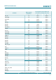
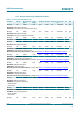
4.4.4 RF front-end control interface
Table 4. RF front-end control interface
Pin Name Supply
No Pad
Power
State
Reset
State
HW State PD State PD Prog
Internal
PU/PD
PU PD
RF_CNTL0_N VIO_RF tristate input output drive low yes weak PU no no
RF Control 0—RF Control Output Low (output)
This pin is used as a configuration pin: CON[0] (input)
See Section 4.5 "Configuration pins".
RF_CNTL1_P VIO_RF tristate input output drive high yes weak PU no no
RF Control 1—RF Control Output High (output)
RF_CNTL2_N VIO_RF tristate input output drive low yes weak PU no no
RF Control 2—RF Control Output Low (output)
This pin is used as a configuration pin: CON[1] (input)
See Section 4.5 "Configuration pins".
RF_CNTL3_P VIO_RF tristate input output drive high yes weak PU no no
RF Control 3—RF Control Output High (output)
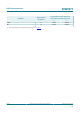
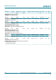
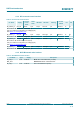
4.4.5 Wi-Fi/Bluetooth radio interface
Table 5. Wi-Fi/Bluetooth radio interface
Pin Name Type Supply Description
RF_TR_2 /
BRF_ANT
A, I/O AVDD18 Wi-Fi: Wi-Fi Transmit/Receive (2.4 GHz)
Bluetooth: Bluetooth Transmit/Receive
RF_TR_5 A, I/O AVDD18 Wi-Fi Transmit/Receive (5 GHz)