
Datasheet


NXP Semiconductors
88W8977
2.4 GHz/5 GHz Dual-band 1x1 Wi-Fi 4
®
and Bluetooth
®
5 Combo SoC
88W8977 All information provided in this document is subject to legal disclaimers. © NXP B.V. 2020. All rights reserved.
Product short data sheet Rev. 1 — 13 July 2020
16 / 81
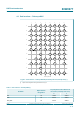
4.4 Pin description
4.4.1 Pin types
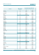
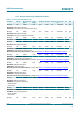
Table 2. Pin types
Pin type Description
I/O Digital input/output
I Digital input
O Digital output
A, I Analog input
A,O Analog output
NC No connect
DNC Do not connect
Power Power
Ground Ground
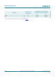
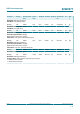
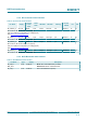
4.4.2 Pin states
The pin state information provided in this section is defined as follows:
• After firmware is downloaded, pads like GPIO and RF control are programmed in
functional mode per the functionality of the pins
• The Hardware State (HW State) at power-on may differ based on the pin muxing/strap
setting. The HW State is the pin state at power-on after boot code finishes and before
firmware download begins (firmware may change the pin state). For example, for
UART_RTSn and UART_SOUT, the boot code will enable the UART interface, making
the HW states output high and output low, respectively.
• PD State denotes the power-down state in default configuration. Many pads have
programmable power-down values, which can be set by firmware.
• PD Prog denotes whether the power-down state is programmable or not
• PU denotes whether the pull-up is programmable or not
• PD denotes whether the pull-down is programmable or not
• Pull-up and pull-down are only effective when the pad is in input mode.
• For SDIO, once the command is received from the host, the pads are configured
accordingly