
Datasheet


NXP Semiconductors
88W8977
2.4 GHz/5 GHz Dual-band 1x1 Wi-Fi 4
®
and Bluetooth
®
5 Combo SoC
88W8977 All information provided in this document is subject to legal disclaimers. © NXP B.V. 2020. All rights reserved.
Product short data sheet Rev. 1 — 13 July 2020
10 / 81
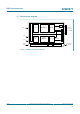
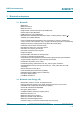
4 Pin information
4.1 Signal diagram
Note: Signals may be muxed. See Pin description (BRF_ANT signal is muxed with
RF_TR_2 pin; Bluetooth external coexistence signals are muxed with both GPIO[11:8]
and SD_DAT[3:0] pins).
88W8977
PCM interface
PCM_SYNC
PCM_CLK
PCM_DOUT
PCM_DIN
PCM_MCLK
PDn
Clock interface
RF front-end control
interface
JTAG interface
JTAG_TDI
JTAG_TCK
JTAG_TDO
JTAG_TMS
Power management
interface
DVSC[1]
DVSC[0]
Wi-Fi radio interface
RF_TR_2
RF_TR_5
SLP_CLK_IN
XTAL_OUT
XTAL_IN
XOSC_EN
Power-down
Bluetooth external
coexistence interface
UART_LTE_SIN
UART_LTE_SOUT
LTE external
coexistence interface
BT_GRANTn
BT_FREQ
BT_STATE
BT_REQ
RF_CNTL0_N
RF_CNTL1_P
RF_CNTL2_N
RF_CNTL3_P
UART interface
UART_SIN
UART_SOUT
UART_RTSn
UART_CTSn
SDIO interface
SD_CLK
SD_CMD
SD_DAT[3:0]
Bluetooth radio interface
BRF_ANT
(shared with RF_TR_2 pin)
GPIO interface
GPIO[15:0]
Figure 3. 88W8977 signal diagram