INTEGRATED CIRCUITS DATA SHEET For a complete data sheet, please also download: • The IC06 74HC/HCT/HCU/HCMOS Logic Family Specifications • The IC06 74HC/HCT/HCU/HCMOS Logic Package Information • The IC06 74HC/HCT/HCU/HCMOS Logic Package Outlines 74HCU04 Hex inverter Product specification File under Integrated Circuits, IC06 September 1993
Philips Semiconductors Product specification Hex inverter 74HCU04 FEATURES • Output capability: standard • ICC category: SSI GENERAL DESCRIPTION The 74HCU04 is a high-speed Si-gate CMOS device and is pin compatible with low power Schottky TTL (LSTTL). It is specified in compliance with JEDEC standard no. 7A. The 74HCU04 is a general purpose hex inverter.
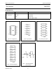
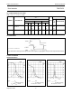
Philips Semiconductors Product specification Hex inverter 74HCU04 PIN DESCRIPTION PIN NO. SYMBOL NAME AND FUNCTION 1, 3, 5, 9, 11, 13 1A to 6A data inputs 2, 4, 6, 8, 10, 12 1Y to 6Y data outputs 7 GND ground (0 V) 14 VCC positive supply voltage Fig.1 Pin configuration. Fig.4 Functional diagram. September 1993 Fig.2 Logic symbol. Fig.5 Schematic diagram (one inverter). 3 Fig.3 IEC logic symbol.
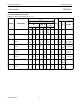
Philips Semiconductors Product specification Hex inverter 74HCU04 DC CHARACTERISTICS FOR 74HCU Voltages are referenced to GND (ground = 0 V) Tamb(°C) TEST CONDITIONS 74HCU SYMBOL PARAMETER +25 min. typ. -40 to +85 UNIT V CC (V) VI OTHER max. min. max. min. max. VIH HIGH level input voltage 1.7 3.6 4.8 1.4 2.6 3.4 VIL LOW level input voltage 0.6 1.9 2.6 VOH HIGH level output voltage 1.8 4.0 5.5 VOH HIGH level output voltage 3.98 4.32 5.48 5.
Philips Semiconductors Product specification Hex inverter 74HCU04 AC CHARACTERISTICS FOR 74HCU GND = 0 V; tr = tf = 6 ns; CL = 50 pF Tamb (°C) TEST CONDITIONS 74HCU SYMBOL PARAMETER +25 min. typ. -40 to +85 max. min. max. −40 to +125 min. UNIT VCC (V) WAVEFORMS max. tPHL/ tPLH propagation delay nA to nY 19 7 6 70 14 12 90 18 15 105 21 18 ns 2.0 4.5 6.0 Fig.6 tTHL/ tTLH output transition time 19 7 6 75 15 13 95 19 16 110 22 19 ns 2.0 4.5 6.0 Fig.
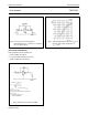
Philips Semiconductors Product specification Hex inverter 74HCU04 Fig.10 Test set-up for measuring forward transconductance gfs = dio/dvi at vo is constant (see also graph Fig.11). Fig.11 Typical forward transconductance gfs as a function of the supply voltage VCC at Tamb = 25°C. APPLICATION INFORMATION Some applications for the “HCU04” are: • Linear amplifier (see Fig.12) • In crystal oscillator designs (see Fig.13) • Astable multivibrator (see Fig.14) ZL > 10 kΩ; AOL = 20 (typ.
Philips Semiconductors Product specification Hex inverter 74HCU04 1 1 f = --- ≈ -----------------T 2.2 RC C1 = 47 pF (typ.) C2 = 33 pF (typ.) R1 = 1 to 10 MΩ (typ.) R2 optimum value depends on the frequency and required stability against changes in VCC or average minimum ICC (ICC is typically 5 mA at VCC = 5 V and f = 10 MHz). RS ≈ 2 × R. The average ICC (mA) is approximately 3.5 + 0.05 × f (MHz) × C (pF) at VCC = 5.0 V (for more information refer to “DESIGNERS GUIDE”). Fig.