
Datasheet


Table Of Contents
- Section 1. General Description
- 1.1 Contents
- 1.2 Introduction
- 1.3 Features
- 1.3.1 Standard Features of the MC68HC908GP20
- 1.3.2 Features of the CPU08
- 1.4 MCU Block Diagram
- 1.5 Pin Assignments
- 1.6 Pin Functions
- 1.6.1 Power Supply Pins (VDD and VSS)
- 1.6.2 Oscillator Pins (OSC1 and OSC2)
- 1.6.3 External Reset Pin (RST)
- 1.6.4 External Interrupt Pin (IRQ)
- 1.6.5 CGM Power Supply Pins (VDDA and VSSA)
- 1.6.6 External Filter Capacitor Pin (CGMXFC)
- 1.6.7 Analog Power Supply Pins (VDDAD and VSSAD)
- 1.6.8 ADC Voltage Reference High Pin (VREFH)
- 1.6.9 ADC Voltage Reference Low Pin (VREFL)
- 1.6.10 Port A Input/Output (I/O) Pins (PTA7/KBD7-PTA0/KBD0)
- 1.6.11 Port B I/O Pins (PTB7/AD7-PTB0/AD0)
- 1.6.12 Port C I/O Pins (PTC6-PTC0)
- 1.6.13 Port D I/O Pins (PTD7/T2CH1-PTD0/SS)
- 1.6.14 Port E I/O Pins (PTE1/RxD-PTE0/TxD)
- Section 2. Memory Map
- Section 3. Low-Power Modes
- 3.1 Contents
- 3.2 Introduction
- 3.2.1 Wait Mode
- 3.2.2 Stop Mode
- 3.3 Analog-to-Digital Converter (ADC)
- 3.3.1 Wait Mode
- 3.3.2 Stop Mode
- 3.4 Break Module (BRK)
- 3.4.1 Wait Mode
- 3.4.2 Stop Mode
- 3.5 Central Processor Unit (CPU)
- 3.5.1 Wait Mode
- 3.5.2 Stop Mode
- 3.6 Clock Generator Module (CGM)
- 3.6.1 Wait Mode
- 3.6.2 Stop Mode
- 3.7 Computer Operating Properly Module (COP)
- 3.7.1 Wait Mode
- 3.7.2 Stop Mode
- 3.8 External Interrupt Module (IRQ)
- 3.8.1 Wait Mode
- 3.8.2 Stop Mode
- 3.9 Keyboard Interrupt Module (KBI)
- 3.9.1 Wait Mode
- 3.9.2 Stop Mode
- 3.10 Low-Voltage Inhibit Module (LVI)
- 3.10.1 Wait Mode
- 3.10.2 Stop Mode
- 3.11 Serial Communications Interface Module (SCI)
- 3.11.1 Wait Mode
- 3.11.2 Stop Mode
- 3.12 Serial Peripheral Interface Module (SPI)
- 3.12.1 Wait Mode
- 3.12.2 Stop Mode
- 3.13 Timer Interface Module (TIM1 and TIM2)
- 3.13.1 Wait Mode
- 3.13.2 Stop Mode
- 3.14 Timebase Module (TBM)
- 3.14.1 Wait Mode
- 3.14.2 Stop Mode
- 3.15 Exiting Wait Mode
- 3.16 Exiting Stop Mode
- Section 4. Resets and Interrupts
- Section 5. Analog-to-Digital Converter (ADC)
- 5.1 Contents
- 5.2 Introduction
- 5.3 Features
- 5.4 Functional Description
- 5.4.1 ADC Port I/O Pins
- 5.4.2 Voltage Conversion
- 5.4.3 Conversion Time
- 5.4.4 Conversion
- 5.4.5 Accuracy and Precision
- 5.5 Interrupts
- 5.6 Low-Power Modes
- 5.6.1 Wait Mode
- 5.6.2 Stop Mode
- 5.7 I/O Signals
- 5.7.1 ADC Analog Power Pin (VDDAD)/ADC Voltage Reference High Pin (VREFH)
- 5.7.2 ADC Analog Ground Pin (VSSAD)/ADC Voltage Reference Low Pin (VREFL)
- 5.7.3 ADC Voltage In (ADVIN)
- 5.8 I/O Registers
- 5.8.1 ADC Status and Control Register
- 5.8.2 ADC Data Register
- 5.8.3 ADC Clock Register
- Section 6. Break Module (BRK)
- 6.1 Contents
- 6.2 Introduction
- 6.3 Features
- 6.4 Functional Description
- 6.4.1 Flag Protection During Break Interrupts
- 6.4.2 CPU During Break Interrupts
- 6.4.3 TIMI and TIM2 During Break Interrupts
- 6.4.4 COP During Break Interrupts
- 6.5 Low-Power Modes
- 6.5.1 Wait Mode
- 6.5.2 Stop Mode
- 6.6 Break Module Registers
- 6.6.1 Break Status and Control Register
- 6.6.2 Break Address Registers
- 6.6.3 Break Status Register
- 6.6.4 Break Flag Control Register
- Section 7. Clock Generator Module (CGMC)
- 7.1 Contents
- 7.2 Introduction
- 7.3 Features
- 7.4 Functional Description
- 7.4.1 Crystal Oscillator Circuit
- 7.4.2 Phase-Locked Loop Circuit (PLL)
- 7.4.3 PLL Circuits
- 7.4.4 Acquisition and Tracking Modes
- 7.4.5 Manual and Automatic PLL Bandwidth Modes
- 7.4.6 Programming the PLL
- 7.4.7 Special Programming Exceptions
- 7.4.8 Base Clock Selector Circuit
- 7.4.9 CGMC External Connections
- 7.5 I/O Signals
- 7.5.1 Crystal Amplifier Input Pin (OSC1)
- 7.5.2 Crystal Amplifier Output Pin (OSC2)
- 7.5.3 External Filter Capacitor Pin (CGMXFC)
- 7.5.4 PLL Analog Power Pin (Vdda)
- 7.5.5 PLL Analog Ground Pin (Vssa)
- 7.5.6 Oscillator Enable Signal (SIMOSCEN)
- 7.5.7 Oscillator Stop Mode Enable Bit (OSCSTOPENB)
- 7.5.8 Crystal Output Frequency Signal (CGMXCLK)
- 7.5.9 CGMC Base Clock Output (CGMOUT)
- 7.5.10 CGMC CPU Interrupt (CGMINT)
- 7.6 CGMC Registers
- 7.6.1 PLL Control Register
- 7.6.2 PLL Bandwidth Control Register
- 7.6.3 PLL Multiplier Select Register High
- 7.6.4 PLL Multiplier Select Register Low
- 7.6.5 PLL VCO Range Select Register
- 7.6.6 PLL Reference Divider Select Register
- 7.7 Interrupts
- 7.8 Special Modes
- 7.8.1 Wait Mode
- 7.8.2 Stop Mode
- 7.8.3 CGMC During Break Interrupts
- 7.9 Acquisition/Lock Time Specifications
- 7.9.1 Acquisition/Lock Time Definitions
- 7.9.2 Parametric Influences on Reaction Time
- 7.9.3 Choosing a Filter
- Section 8. Configuration Register (CONFIG)
- Section 9. Computer Operating Properly (COP)
- 9.1 Contents
- 9.2 Introduction
- 9.3 Functional Description
- 9.4 I/O Signals
- 9.4.1 CGMXCLK
- 9.4.2 STOP Instruction
- 9.4.3 COPCTL Write
- 9.4.4 Power-On Reset
- 9.4.5 Internal Reset
- 9.4.6 Reset Vector Fetch
- 9.4.7 COPD (COP Disable)
- 9.4.8 COPRS (COP Rate Select)
- 9.5 COP Control Register
- 9.6 Interrupts
- 9.7 Monitor Mode
- 9.8 Low-Power Modes
- 9.8.1 Wait Mode
- 9.8.2 Stop Mode
- 9.9 COP Module During Break Mode
- Section 10. Central Processor Unit (CPU)
- 10.1 Contents
- 10.2 Introduction
- 10.3 Features
- 10.4 CPU Registers
- 10.4.1 Accumulator
- 10.4.2 Index Register
- 10.4.3 Stack Pointer
- 10.4.4 Program Counter
- 10.4.5 Condition Code Register
- 10.5 Arithmetic/Logic Unit (ALU)
- 10.6 Low-Power Modes
- 10.6.1 Wait Mode
- 10.6.2 Stop Mode
- 10.7 CPU During Break Interrupts
- 10.8 Instruction Set Summary
- 10.9 Opcode Map
- Section 11. FLASH Memory
- 11.1 Contents
- 11.2 Introduction
- 11.3 Functional Description
- 11.4 FLASH Control Register
- 11.5 Charge Pump
- 11.5.1 FLASH Charge Pump Frequency Control
- 11.5.2 Voltage Regulator
- 11.6 FLASH Erase Operation
- 11.7 FLASH Program/Margin Read Operation
- 11.8 FLASH Block Protection
- 11.9 FLASH Block Protect Register
- 11.10 Wait Mode
- 11.11 Stop Mode
- Section 12. External Interrupt (IRQ)
- Section 13. Keyboard Interrupt Module (KBI)
- Section 14. Low-Voltage Inhibit (LVI)
- Section 15. Monitor ROM (MON)
- Section 16. Input/Output (I/O) Ports
- 16.1 Contents
- 16.2 Introduction
- 16.3 Port A
- 16.3.1 Port A Data Register
- 16.3.2 Data Direction Register A
- 16.3.3 Port A Input Pullup Enable Register
- 16.4 Port B
- 16.4.1 Port B Data Register
- 16.4.2 Data Direction Register B
- 16.5 Port C
- 16.5.1 Port C Data Register
- 16.5.2 Data Direction Register C
- 16.5.3 Port C Input Pullup Enable Register
- 16.6 Port D
- 16.6.1 Port D Data Register
- 16.6.2 Data Direction Register D
- 16.6.3 Port D Input Pullup Enable Register
- 16.7 Port E
- 16.7.1 Port E Data Register
- 16.7.2 Data Direction Register E
- Section 17. Random-Access Memory (RAM)
- Section 18. Serial Communications Interface Module (SCI)
- 18.1 Contents
- 18.2 Introduction
- 18.3 Features
- 18.4 Pin Name Conventions
- 18.5 Functional Description
- 18.5.1 Data Format
- 18.5.2 Transmitter
- 18.5.3 Receiver
- 18.6 Low-Power Modes
- 18.6.1 Wait Mode
- 18.6.2 Stop Mode
- 18.7 SCI During Break Module Interrupts
- 18.8 I/O Signals
- 18.8.1 PTE0/TxD (Transmit Data)
- 18.8.2 PTE1/RxD (Receive Data)
- 18.9 I/O Registers
- 18.9.1 SCI Control Register 1
- 18.9.2 SCI Control Register 2
- 18.9.3 SCI Control Register 3
- 18.9.4 SCI Status Register 1
- 18.9.5 SCI Status Register 2
- 18.9.6 SCI Data Register
- 18.9.7 SCI Baud Rate Register
- Section 19. System Integration Module (SIM)
- 19.1 Contents
- 19.2 Introduction
- 19.3 SIM Bus Clock Control and Generation
- 19.3.1 Bus Timing
- 19.3.2 Clock Startup from POR or LVI Reset
- 19.3.3 Clocks in Stop Mode and Wait Mode
- 19.4 Reset and System Initialization
- 19.4.1 External Pin Reset
- 19.4.2 Active Resets from Internal Sources
- 19.5 SIM Counter
- 19.5.1 SIM Counter During Power-On Reset
- 19.5.2 SIM Counter During Stop Mode Recovery
- 19.5.3 SIM Counter and Reset States
- 19.6 Exception Control
- 19.6.1 Interrupts
- 19.6.2 Reset
- 19.6.3 Break Interrupts
- 19.6.4 Status Flag Protection in Break Mode
- 19.7 Low-Power Modes
- 19.7.1 Wait Mode
- 19.7.2 Stop Mode
- 19.8 SIM Registers
- 19.8.1 SIM Break Status Register
- 19.8.2 SIM Reset Status Register
- 19.8.3 SIM Break Flag Control Register
- Section 20. Serial Peripheral Interface Module (SPI)
- 20.1 Contents
- 20.2 Introduction
- 20.3 Features
- 20.4 Pin Name Conventions and I/O Register Addresses
- 20.5 Functional Description
- 20.5.1 Master Mode
- 20.5.2 Slave Mode
- 20.6 Transmission Formats
- 20.6.1 Clock Phase and Polarity Controls
- 20.6.2 Transmission Format When CPHA = 0
- 20.6.3 Transmission Format When CPHA = 1
- 20.6.4 Transmission Initiation Latency
- 20.7 Queuing Transmission Data
- 20.8 Error Conditions
- 20.8.1 Overflow Error
- 20.8.2 Mode Fault Error
- 20.9 Interrupts
- 20.10 Resetting the SPI
- 20.11 Low-Power Modes
- 20.11.1 Wait Mode
- 20.11.2 Stop Mode
- 20.12 SPI During Break Interrupts
- 20.13 I/O Signals
- 20.13.1 MISO (Master In/Slave Out)
- 20.13.2 MOSI (Master Out/Slave In)
- 20.13.3 SPSCK (Serial Clock)
- 20.13.4 SS (Slave Select)
- 20.13.5 CGND (Clock Ground)
- 20.14 I/O Registers
- 20.14.1 SPI Control Register
- 20.14.2 SPI Status and Control Register
- 20.14.3 SPI Data Register
- Section 21. Timebase Module (TBM)
- Section 22. Timer Interface Module (TIM)
- 22.1 Contents
- 22.2 Introduction
- 22.3 Features
- 22.4 Pin Name Conventions
- 22.5 Functional Description
- 22.5.1 TIM Counter Prescaler
- 22.5.2 Input Capture
- 22.5.3 Output Compare
- 22.5.4 Unbuffered Output Compare
- 22.5.5 Buffered Output Compare
- 22.5.6 Pulse Width Modulation (PWM)
- 22.5.7 Unbuffered PWM Signal Generation
- 22.5.8 Buffered PWM Signal Generation
- 22.5.9 PWM Initialization
- 22.6 Interrupts
- 22.7 Low-Power Modes
- 22.7.1 Wait Mode
- 22.7.2 Stop Mode
- 22.8 TIM During Break Interrupts
- 22.9 I/O Signals
- 22.10 I/O Registers
- 22.10.1 TIM Status and Control Register
- 22.10.2 TIM Counter Registers
- 22.10.3 TIM Counter Modulo Registers
- 22.10.4 TIMA Counter Registers
- 22.10.5 TIM Channel Status and Control Registers
- 22.10.6 TIM Channel Registers
- Section 23. Preliminary Electrical Specifications
- 23.1 Contents
- 23.2 Introduction
- 23.3 Absolute Maximum Ratings
- 23.4 Functional Operating Range
- 23.5 Thermal Characteristics
- 23.6 5.0-V DC Electrical Characteristics
- 23.7 3.0-V DC Electrical Characteristics
- 23.8 5.0-V Control Timing
- 23.9 3.0-V Control Timing
- 23.10 Output High-Voltage Characteristics
- 23.11 Output Low-Voltage Characteristics
- 23.12 Typical Supply Currents
- 23.13 ADC Characteristics
- 23.14 5.0-V SPI Characteristics
- 23.15 3.0-V SPI Characteristics
- 23.16 Timer Interface Module Characteristics
- 23.17 Clock Generation Module Characteristics
- 23.17.1 CGM Component Specifications
- 23.17.2 CGM Electrical Specifications
- 23.18 Memory Characteristics
- Section 24. Mechanical Specifications
- Section 25. Ordering Information
MC68HC908GP20 — Rev 2.1 Advance Information
Freescale Semiconductor 231
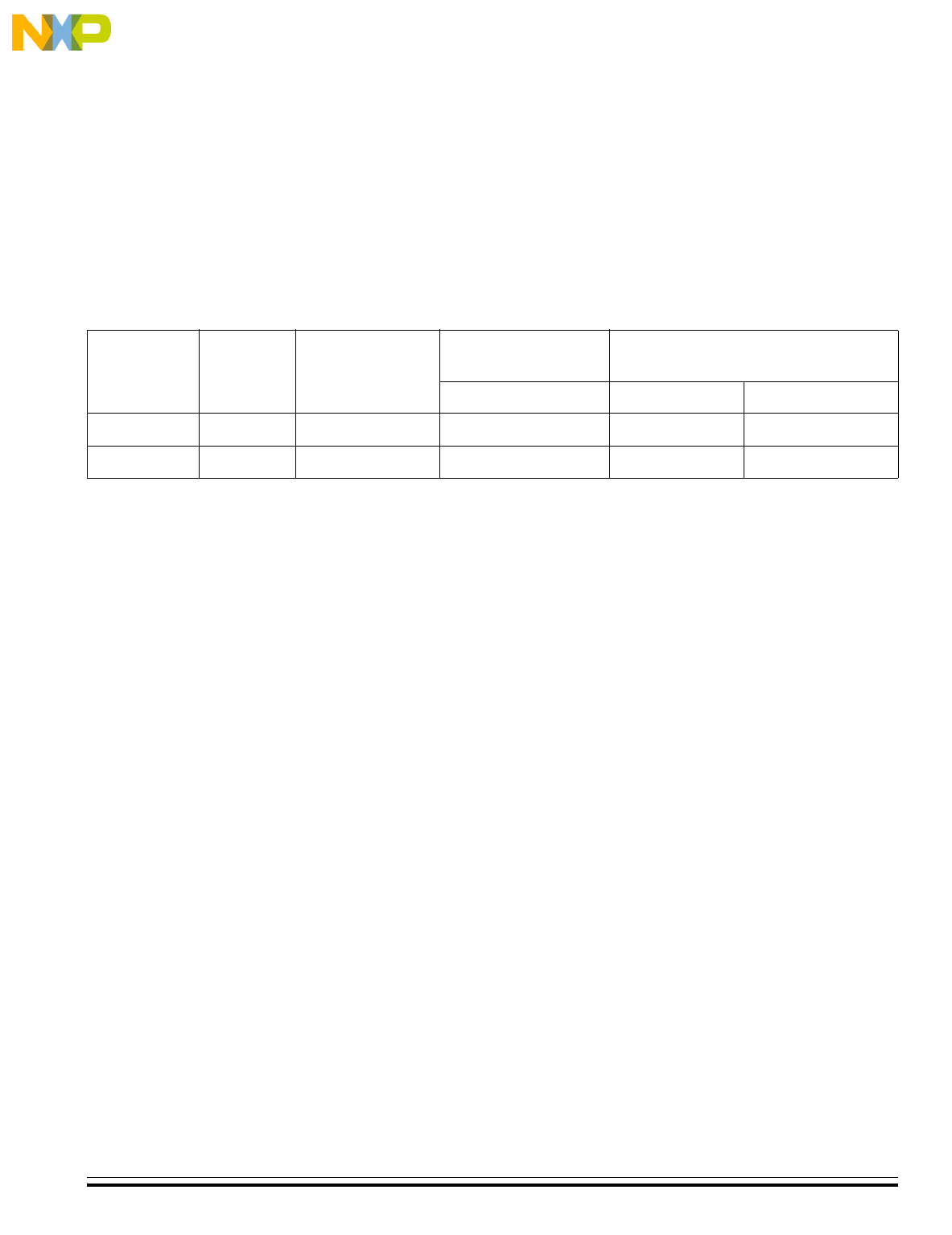
When bit DDRBx is a logic 1, reading address $0001 reads the PTBx
data latch. When bit DDRBx is a logic 0, reading address $0001 reads
the voltage level on the pin. The data latch can always be written,
regardless of the state of its data direction bit. Table 16-3 summarizes
the operation of the port B pins.
Table 16-3. Port B Pin Functions
DDRB Bit PTB Bit I/O Pin Mode
Accesses
to DDRB
Accesses to PTB
Read/Write Read Write
0X
(1)
Input, Hi-Z
(2)
DDRB7–DDRB0 Pin PTB7–PTB0
(3)
1 X Output DDRB7–DDRB0 PTB7–PTB0 PTB7–PTB0
Notes:
1. X = Don’t care
2. Hi-Z = High impedance
3. Writing affects data register, but does not affect input.