
Datasheet


TDA8025_1 © NXP B.V. 2009. All rights reserved.
Product data sheet Rev. 01 — 6 April 2009 9 of 38
NXP Semiconductors
TDA8025
IC card interface
8.2.3 V
DD(INTREGD)
voltage supervisor with pin PORADJ connected to V
DD(INTF)
The TDA8025 remains in inactive mode irrespective of the levels on the command lines
when
• V
DD(INTREGD)
is less than V
th
+V
hys
(on pin V
DD(INTREGD)
)
• Pin PORADJ (monitoring V
DD(INTF)
) is less than V
th
+V
hys
In both cases, this lasts for the duration of t
w(POR)
after V
DD(INTREGD)
(on pin V
DD(INTREGD)
)
and V
DD(INTF)
(on pin V
DD(INTF)
) have reached a level higher than V
th
+V
hys
. Two threshold
voltages (V
th
) are set by the hardware as follows:
• V
DD(INTREGD)
threshold voltage: is set to the minimum supply voltage (2.7 V) specified
for the digital part of the TDA8025
• V
DD(INTF)
threshold voltage: is set to 1.24 V; see Table 8 on page 23 for detailed
information.
8.2.4 V
DD(INTF)
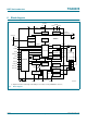
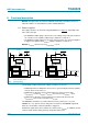
voltage supervisor with external divider on pin PORADJ
An external resistor bridge can be used to divide V
DD(INTF)
on pin PORADJ to adapt the
detection threshold when monitoring the microcontroller interface supply voltage.
Connecting the external resistor bridge as illustrated in Figure 4 on page 8 (R1 connected
to V
DD(INTF)
and R2 connected to GND) to pin PORADJ overrides the internal threshold
voltage V
th
on pin V
DD(INTF)
.
The threshold voltage on pin V
DD(INTF)
is calculated as follows:
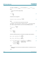
(1)
where
• V
bg
is the bandgap voltage
When the resistor bridge is not used, pin PORADJ must be connected to pin V
DD(INTF)
.
8.2.4.1 R1 and R2 resistor value calculation
This section describes how to calculate the values for resistors R1 and R2, taking into
account the IC detector threshold spread and the external resistance, while ensuring
reliable activation.
If for example, the controller is supplied by a regulator at 3.3 V ± 20 %. Activation can be
triggered above V
DD(INTF)
= 3.3 V − 20 % (in this example 2.64 V). This activation
threshold is defined as V
DD(INTF)actmin
; i.e. the minimum value of V
DD(INTF)
above which
activation can always be triggered.
In addition to this external input, activation is permitted provided all the following
conditions are met (see Table 8 on page 23): card presence, IC temperature, V
DD(INTF)
and V
DD(INTREGD)
supplies, etc.
V
th
on pin V
DD INTF()
V
bg
1R+ 1
R2
----------------
=