
Datasheet


TDA8025_1 © NXP B.V. 2009. All rights reserved.
Product data sheet Rev. 01 — 6 April 2009 7 of 38
NXP Semiconductors
TDA8025
IC card interface
8. Functional description
Remark: Throughout this document the ISO7816 terminology conventions have been
adhered to and it is assumed that the reader is familiar with these.
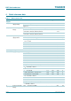
8.1 Power supplies
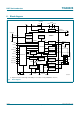
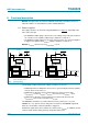
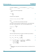
Two supply selections can be made using pin CONFIG (see Figure 3) depending on the
active state of the pin:
• pin CONFIG is LOW: supply is pin V
DDI(REG)
. The voltage range of the pin is between
3.6 V and 5.5 V. The regulator output range is between 3 V and 3.6 V.
• pin CONFIG is HIGH: supply pins V
DDI(REG)
and V
DD(INTREGD)
are connected together
to bypass the regulator. Pin V
DDI(REG)
voltage is between 3 V and 3.6 V.
Remark: V
DD(INTF)
must not exceed V
DD(INTREGD)
+ 0.3 V.
The following examples illustrate the voltage restrictions for V
DD(INTF)
.
• CONFIG pin driven to GND: when V
DD(INTREGD)
is generated by the internal regulator,
V
DD(INTF)
must not exceed 3.3 V.
• CONFIG pin is driven by V
DDI(REG)
without V
DD(INTF)
tied to V
DDI(REG)
while
V
DD(INTREGD)
is tied to V
DDI(REG)
: V
DD(INTF)
must not exceed V
DDI(REG)
+ 0.3 V.
• CONFIG pin is driven by V
DDI(REG)
with V
DD(INTF)
tied to both V
DDI(REG)
and
V
DD(INTREGD)
: there no are restrictions for V
DD(INTF)
.
The TDA8025 is held in the reset state until V
DD(INTREGD)
reaches V
th
+V
hys
and
PORADJ V
th
+V
hys
plus the t
w(POR)
delay. If the V
DD(INTREGD)
and PORADJ signals fall
below V
th
, an automatic contact deactivation is triggered.
All interface signals to the microcontroller are referenced to V
DD(INTF)
. In addition, all card
contacts remain inactive during power-up and power-down cycles.
3.6V<V
DDI(REG)
<5.5V 3V<V
DD(INTREGD)
< 3.6 V
Fig 3. Power strategy
001aai959
470 nF
100 nF
10 µF
10 µF
220 nF
REGULATOR
INTERNAL
REFERENCE
VOLTAGE
SENSE
SUPPLY
V
CC
LOOP
18
211620 19
V
DDI(REG)
CONFIGGND
V
DD(INTREGD)
V
CC
14
CGND
001aai960
470 nF
100 nF
10 µF
220 nF
REGULATOR
INTERNAL
REFERENCE
VOLTAGE
SENSE
SUPPLY
V
CC
LOOP
18
211620 19
V
DDI(REG)
CONFIGGND
V
DD(INTREGD)
V
CC
14
CGND