
Datasheet


TDA8025_1 © NXP B.V. 2009. All rights reserved.
Product data sheet Rev. 01 — 6 April 2009 6 of 38
NXP Semiconductors
TDA8025
IC card interface
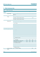
[1] I = input, O = output, I/O = input/output, G = ground and P = power supply.
[2] If pin PRESN or pin PRES is true, the card is considered to be present. During card insertion, debouncing
can occur on these signals. To counter this, the TDA8025 has a built-in debouncing timer (typically 4.5 ms).
[3] Using the internal pull-up resistor connected to pin V
CC
.
[4] Using the internal pull-up resistor connected to pin V
DD(INTF)
.
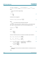
CGND 14 G card signal ground
CLK 15 O card clock (C3)
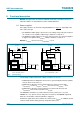
CONFIG 16 I 3.3 V or 5 V core regulator supply voltage selection; see
Figure 3 on
page 7
RST 17 O card reset (C2)
V
CC
18 P card supply (C1); decouple to pin CGND using one 470 nF and one
220 nF capacitor with an Equivalent Series Resistance
(ESR) < 100 mΩ
V
DD(INTREGD)
19 P internally regulated supply voltage
GND 20 G ground
V
DDI(REG)
21 P regulator input supply voltage
RSTIN 22 I microcontroller card reset input; active HIGH
OFFN 23 O NMOS interrupt to microcontroller
[4]
; active LOW; see Section 8.10
on page 19
TEST3 24 O test pin; do not connect to the application
PORADJ 25 I power-on reset threshold adjustment input
[4]
ENCLKIN 26 I enable external clock on pin XTAL1; active HIGH
XTAL2 27 O crystal connection pin; open when used with an external clock source
XTAL1 28 I crystal connection pin; supply reference V
DD(INTREGD)
external clock input; supply reference V
DD(INTF)
I/OUC 29 I/O microcontroller input/output data line
[4]
AUX1UC 30 I/O microcontroller auxiliary 1 input/output data line
[4]
AUX2UC 31 I/O microcontroller auxiliary 2 input/output data line
[4]
TEST4 32 I test pin; connect to GND
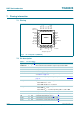
Table 3. Pin description
…continued
Symbol Pin Type
[1]
Description