
Datasheet


TDA8025_1 © NXP B.V. 2009. All rights reserved.
Product data sheet Rev. 01 — 6 April 2009 5 of 38
NXP Semiconductors
TDA8025
IC card interface
7. Pinning information
7.1 Pinning
7.2 Pin description
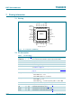
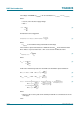
Fig 2. Pin configuration (HVQFN32)
001aai958
TDA8025
Transparent top view
RST
VCC_SEL1
VCC_SEL2
V
CC
CLKDIV1 V
DD(INTREGD)
CLKDIV2 GND
V
DD(INTF)
V
DDI(REG)
TEST2 RSTIN
TEST1 OFFN
CMDVCCN TEST3
PRESN
PRES
I/O
AUX2
AUX1
CGND
CLK
CONFIG
TEST4
AUX2UC
AUX1UC
I/OUC
XTAL1
XTAL2
ENCLKIN
PORADJ
8 17
7 18
6 19
5 20
4 21
3 22
2 23
1 24
9
10
11
12
13
14
15
16
32
31
30
29
28
27
26
25
terminal 1
index area
Table 3. Pin description
Symbol Pin Type
[1]
Description
CMDVCCN 1 I microcontroller start activation sequence input; active LOW
TEST1 2 I test pin; connect to GND
TEST2 3 I test pin; connect to GND
V
DD(INTF)
4 P interface supply voltage
CLKDIV2 5 I sets the clock frequency; used together with pin CLKDIV1;
see
Table 4 on page 12
CLKDIV1 6 I sets the clock frequency; used together pin CLKDIV2; see
Table 4 on
page 12
VCC_SEL1 7 I optional 1.2 V selection control signal:
active HIGH: V
CC
= 1.2 V
active LOW: disables 1.2 V selection
VCC_SEL2 8 I 3 V or 1.8 V selection control signal:
active LOW: V
CC
=3V
active HIGH: V
CC
= 1.8 V when pin VCC_SEL1 is active LOW
PRESN 9 I card presence contact input; active LOW
[2]
PRES 10 I card presence contact input; active HIGH
[2]
I/O 11 I/O card input/output data line (C7)
[3]
AUX2 12 I/O card auxiliary 2 input/output data line (C8)
[3]
AUX1 13 I/O card auxiliary 1 input/output data line (C4)
[3]