
Datasheet


NXP Semiconductors
TDA8025
IC card interface
© NXP B.V. 2009. All rights reserved.
For more information, please visit: http://www.nxp.com
For sales office addresses, please send an email to: salesaddresses@nxp.com
Date of release: 6 April 2009
Document identifier: TDA8025_1
Please be aware that important notices concerning this document and the product(s)
described herein, have been included in section ‘Legal information’.
19. Contents
1 General description . . . . . . . . . . . . . . . . . . . . . . 1
2 Features . . . . . . . . . . . . . . . . . . . . . . . . . . . . . . . 1
3 Applications . . . . . . . . . . . . . . . . . . . . . . . . . . . . 1
4 Quick reference data . . . . . . . . . . . . . . . . . . . . . 2
5 Ordering information . . . . . . . . . . . . . . . . . . . . . 3
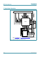
6 Block diagram . . . . . . . . . . . . . . . . . . . . . . . . . . 4
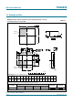
7 Pinning information. . . . . . . . . . . . . . . . . . . . . . 5
7.1 Pinning . . . . . . . . . . . . . . . . . . . . . . . . . . . . . . . 5
7.2 Pin description . . . . . . . . . . . . . . . . . . . . . . . . . 5
8 Functional description . . . . . . . . . . . . . . . . . . . 7
8.1 Power supplies . . . . . . . . . . . . . . . . . . . . . . . . . 7
8.2 Voltage supervisors . . . . . . . . . . . . . . . . . . . . . 8
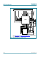
8.2.1 Block diagram . . . . . . . . . . . . . . . . . . . . . . . . . . 8
8.2.2 Description . . . . . . . . . . . . . . . . . . . . . . . . . . . . 8
8.2.3 V
DD(INTREGD)
voltage supervisor with
pin PORADJ connected to V
DD(INTF)
. . . . . . . . 9
8.2.4 V
DD(INTF)
voltage supervisor with external
divider on pin PORADJ. . . . . . . . . . . . . . . . . . . 9
8.2.4.1 R1 and R2 resistor value calculation . . . . . . . . 9
8.3 Clock circuits. . . . . . . . . . . . . . . . . . . . . . . . . . 11
8.4 Input and output circuits . . . . . . . . . . . . . . . . . 13
8.5 Inactive mode . . . . . . . . . . . . . . . . . . . . . . . . . 13
8.6 Activation sequence . . . . . . . . . . . . . . . . . . . . 14
8.7 Active mode . . . . . . . . . . . . . . . . . . . . . . . . . . 17
8.8 Deactivation sequence . . . . . . . . . . . . . . . . . . 18
8.9 V
CC
regulator . . . . . . . . . . . . . . . . . . . . . . . . . 19
8.10 Fault detection . . . . . . . . . . . . . . . . . . . . . . . . 19
9 Limiting values. . . . . . . . . . . . . . . . . . . . . . . . . 22
10 Thermal characteristics. . . . . . . . . . . . . . . . . . 22
11 Characteristics. . . . . . . . . . . . . . . . . . . . . . . . . 23
12 Application information. . . . . . . . . . . . . . . . . . 31
13 Package outline . . . . . . . . . . . . . . . . . . . . . . . . 33
14 Soldering of SMD packages . . . . . . . . . . . . . . 34
14.1 Introduction to soldering . . . . . . . . . . . . . . . . . 34
14.2 Wave and reflow soldering . . . . . . . . . . . . . . . 34
14.3 Wave soldering . . . . . . . . . . . . . . . . . . . . . . . . 34
14.4 Reflow soldering . . . . . . . . . . . . . . . . . . . . . . . 35
15 Abbreviations . . . . . . . . . . . . . . . . . . . . . . . . . . 36
16 Revision history. . . . . . . . . . . . . . . . . . . . . . . . 36
17 Legal information. . . . . . . . . . . . . . . . . . . . . . . 37
17.1 Data sheet status . . . . . . . . . . . . . . . . . . . . . . 37
17.2 Definitions. . . . . . . . . . . . . . . . . . . . . . . . . . . . 37
17.3 Disclaimers . . . . . . . . . . . . . . . . . . . . . . . . . . . 37
17.4 Trademarks. . . . . . . . . . . . . . . . . . . . . . . . . . . 37
18 Contact information. . . . . . . . . . . . . . . . . . . . . 37
19 Contents. . . . . . . . . . . . . . . . . . . . . . . . . . . . . . 38